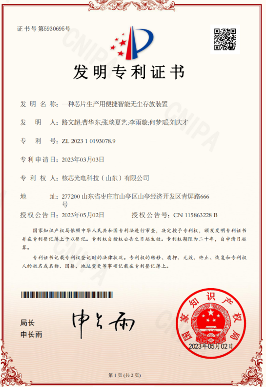
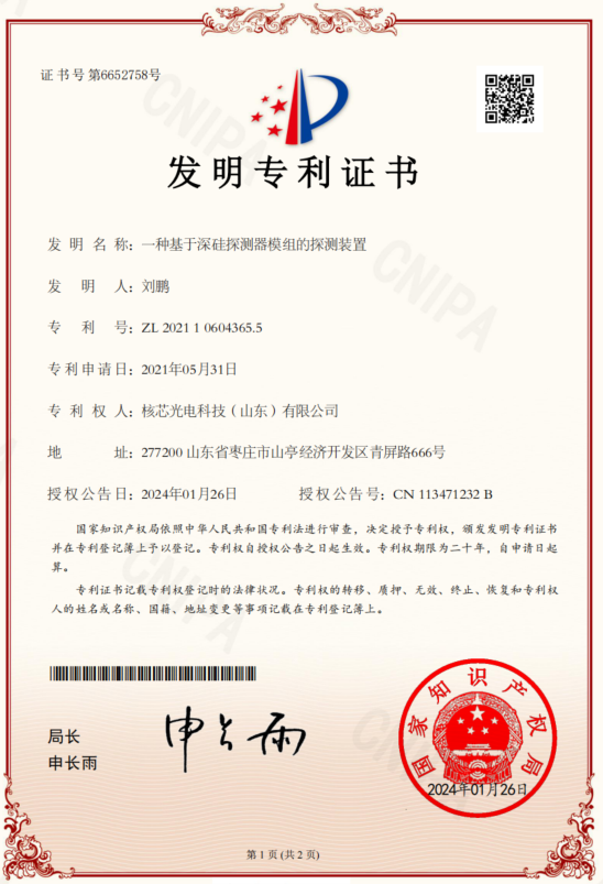
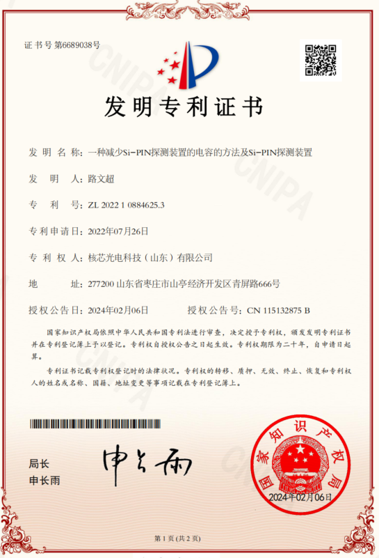
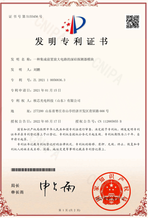
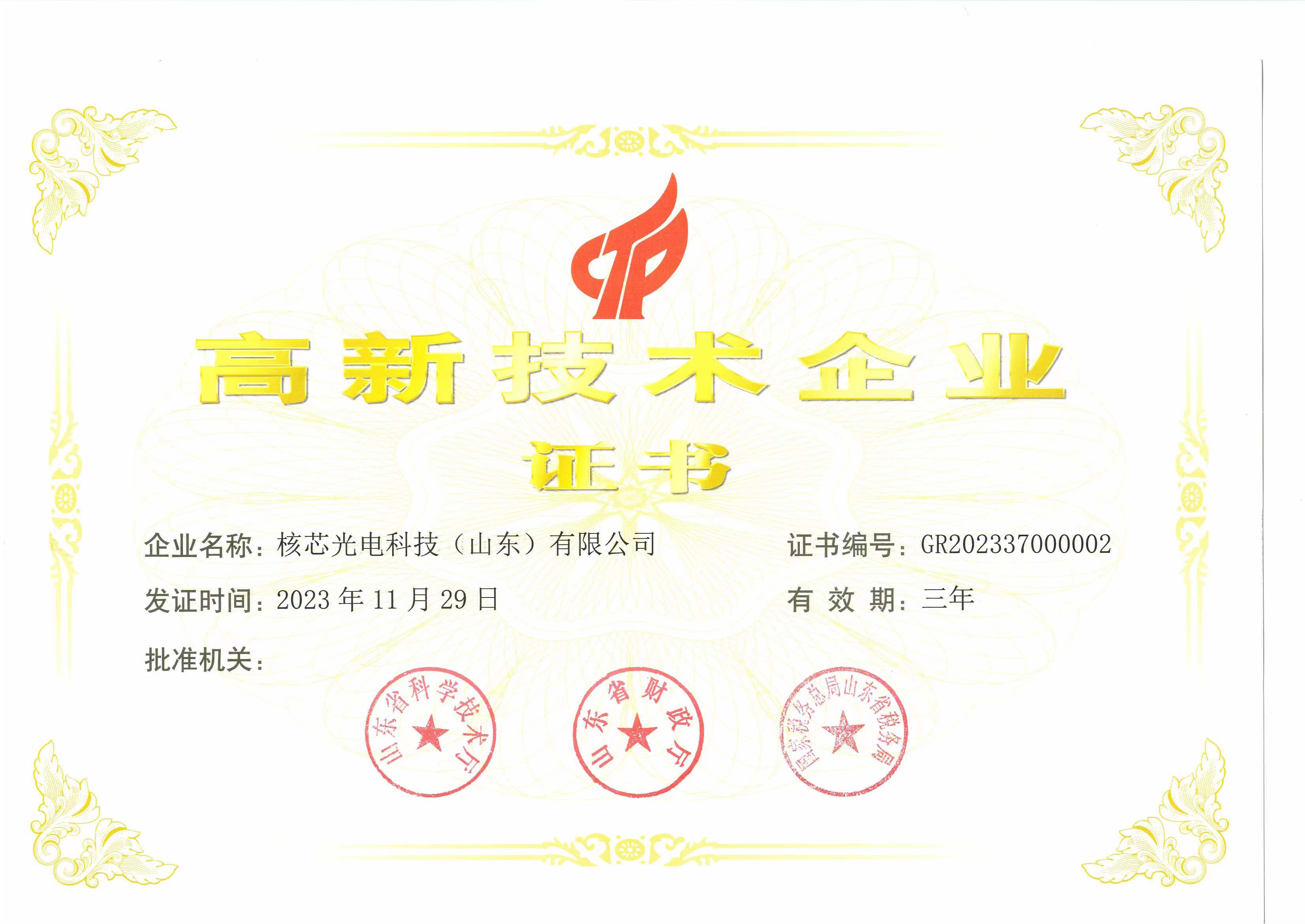
Nuchip photoelectric Technology (Shan Dong) Co., Ltd. was established in September 2019. The company has a registered capital of 53 million yuan, with a planned area of 160 acres and a construction area of 120,000 square meters. The first phase covers 52 acres with a construction area of 53,000 square meters, and the total investment is 650 million yuan.
The company is dedicated to the localization of high-performance photoelectric sensors, aiming to break foreign monopolies. It is a high-tech company in China that possesses the technology for producing high-performance photoelectric sensors with performance indicators meeting international advanced levels. The main products include two categories: 1. photoelectric sensor products, which consist of PIPS products for X-ray and charged particle detection (Si-PIN sensors, silicon drift detectors (SDD), silicon pixel detectors (SPD), silicon micro-strip detectors (SSD), etc.) and PD products for near-infrared, visible, and ultraviolet bands (single pixel, multi-pixel, linear array, area array, etc.), APD and SPAD products; 2. Core component products, including XRF core components, XRD core components, nuclear instrument core components, medical imaging core components, and industrial CT core components.
The application fields of the products include medical equipment, aerospace, security, laser ranging, laser radar, life sciences, pollution detection, analytical instruments, industrial equipment, optical communication, and automotive industries. The products developed by the company’s technical team have replaced those of foreign companies in areas such as space science, nuclear detection, and environmental safety.
The six-inch semiconductor process line includes all semiconductor processing steps such as oxidation, photoetching, ion implantation, and sputtering, along with back-end processing facilities like dicing, die bonding, packaging, and testing. It is equipped with supporting systems for deionized water system, process gases system (high-purity oxygen, nitrogen, helium, etc.), power systems, and waste gas and wastewater treatment systems. This line is primarily used for the R&D of high-performance photoelectric sensor chips, breakthroughs in key technologies, and small-batch production of sensor products (visible light, ultraviolet, X-ray, gamma-ray, charged particles). In the future, it can expand into R&D and small-batch production of silicon ultraviolet sensors and compound semiconductor infrared sensors. The six-inch production line is currently operational and has the technical capabilities for chip design, wafer manufacturing, packaging testing, and component development. It is China’s dedicated silicon semiconductor production line for photoelectric sensors, with product performance indicators evaluated by customers reaching international advanced levels.


