

In the wave of exploration for next-generation electronic technology, the International Center for Quantum Materials at Peking University, in collaboration with Renmin University of China, has successfully prepared wafer-level two-dimensional indium selenide (InSe) semiconductor, bringing a new breakthrough to the semiconductor field. The team led by Professor Liu Kaihui has effectively overcome long-standing challenges in two-dimensional semiconductor manufacturing through the innovative development of a "solid-liquid-solid" growth strategy.
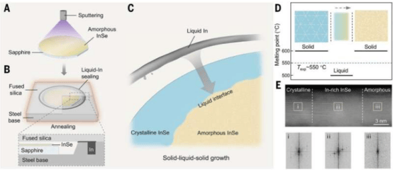
Indium selenide, known as the "golden semiconductor," has attracted much attention due to its low effective mass, high thermal velocity, and suitable bandgap. However, due to the difficulty in precisely controlling the atomic ratio of indium and selenium during the synthesis process, its wafer-level integration has been difficult to achieve. The new strategy developed by Professor Liu Kaihui's team first uses magnetron sputtering to deposit amorphous InSe thin films on sapphire substrates, then encapsulates the wafer with low-melting-point indium. When heated to approximately 550°C, the indium forms a locally indium-rich environment, promoting controlled dissolution and recrystallization at the interface, ultimately forming a uniform single-phase InSe crystal thin film. This method successfully produced a 2-inch wafer, with crystallinity, phase purity, and thickness uniformity reaching high levels in the field of two-dimensional InSe.
Based on these high-quality wafers, the team fabricated large-scale transistor arrays with excellent performance, achieving an electron mobility as high as 287cm²/V·s and an average subthreshold swing of 67mV/dec. These devices exhibit outstanding performance at gate lengths less than 10 nanometers, including reduced drain-induced barrier lowering, lower operating voltage, and enhanced on/off current ratio. Notably, their delay and energy-delay product surpass the 2037 IRDS predictions, positioning InSe ahead of silicon in future chip performance competition. This breakthrough in two-dimensional indium selenide preparation technology opens a new path for the research and development of next-generation high-performance, low-power chips, and is expected to be widely applied in cutting-edge fields such as artificial intelligence, autonomous driving, and smart terminals in the future. Reviewers of the journal Science described this work as "a progress in the field of crystal growth."