

The future of digital computing and communication may be led by the deep integration of electronics and photonics. Electronics uses electricity to manipulate data, while photonics uses light to manipulate data. The combination of the two can not only drive exponential growth in global data traffic but also improve energy utilization efficiency. "Integrating photonics with electronics in the same package is a key direction for transistor development in the 21st century," said Lionel Kimerling, Professor in the Department of Materials Science and Engineering at MIT.
Against this backdrop, the new MIT research team FUTUR-IC has emerged. The team leader and Principal Research Scientist at the Materials Research Laboratory, Anu Agarwal, stated: "Our goal is to build a resource-efficient microchip industry value chain." To achieve this objective, FUTUR-IC researchers—including Agarwal and Kimerling—have developed a new method for co-packaging photonic chips with electronic chips, addressing multiple challenges in current processes. The advantage of the new co-packaged device lies in its ability to utilize existing equipment in traditional electronic foundries and employ lower-cost passive alignment processes for production, promising cost-effectiveness. Earlier this year, a paper on this device (which has been patented) appeared on the cover of Advanced Engineering Materials. The lead author of the paper, Drew Weninger, presented related work at the International Microelectronics Symposium and received the Best Student Paper Award.
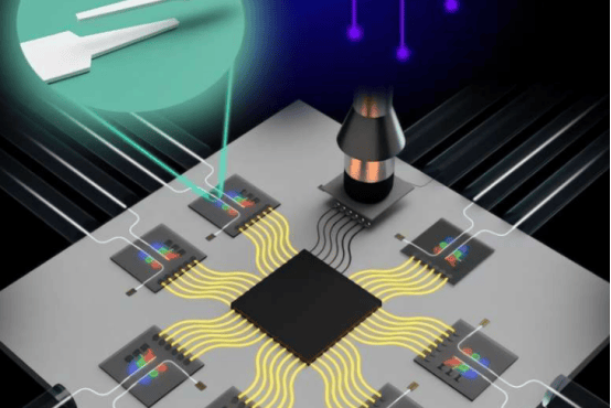
The new device, called the "evanescent coupler," provides greater flexibility for optical fiber connections in electronic-photonic packaging. Agarwal explained: "Traditional couplers have only one coupling point with strict alignment tolerances. Our new coupler features a larger interaction length, increasing alignment tolerance." This means robots can passively assemble the final integrated circuit without the need for active laser alignment, allowing more light to pass through with minimal loss. In addition, the coupler enables vertical optical transmission between multi-layer chips—an important breakthrough, as routing light out of the horizontal plane has been extremely challenging. Drew Weninger stated: "The new coupler allows light to jump between stacked chips." Luigi Ranno summarized: "The packaging design we developed is reliable, has large alignment tolerance, low light loss, high space utilization, and possesses all the characteristics required for efficient and functional interconnection."