

A research team led by Associate Professor Yui Yokota and Professor Akira Yoshikawa from the Institute for Materials Research at Tohoku University in Japan has successfully developed a new high-temperature single crystal growth technology. The technology uses a tungsten crucible to achieve crystal growth above 2200 degrees Celsius, breaking through the heat resistance limitations of existing semiconductor materials. This breakthrough research was published in the journal Scientific Reports.
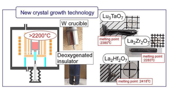
Currently, single crystal materials used in semiconductors, electronic devices, and optical devices typically use iridium or platinum as manufacturing materials. However, the melting points of these metals are below 2200 degrees Celsius, making them unable to meet the application requirements in higher temperature environments. Yui Yokota pointed out: "The reason tungsten has not been successful before is that it easily reacts with oxides and may mix into the crystal, thereby contaminating the final product."
The research team successfully suppressed unnecessary chemical reactions and contamination problems through innovative technology, clarified the relevant reaction mechanisms, and developed effective suppression methods. This single crystal growth technology not only solves the material stability problem in high-temperature environments, but also successfully developed high-density single crystals with performance surpassing existing scintillators.
This single crystal growth technology is of great significance for the discovery of new materials and the mass production of high-temperature oxide single crystals. Akira Yoshikawa said: "These results are exciting because it means we can create a large number of new materials suitable for a wide range of applications." Currently, with the support of the Japan Science and Technology Agency, the technology is being developed for mass production schemes.
The breakthrough in high-temperature single crystal growth technology will accelerate the development of semiconductors, optical materials, scintillators, and piezoelectric materials. In medical applications, the crystals produced by this technology can be used in PET equipment, helping to shorten the time for early cancer detection.