Infineon Technologies of Germany Produces 300 mm Silicon Carbide Power Device Wafers in Austria
en.Wedoany.com Reported - On November 9, German semiconductor manufacturer Infineon successfully fabricated functional power semiconductor devices from 300 mm silicon carbide wafers at its Villach fab in Austria, completing process feasibility validation of this wafer size for silicon carbide in an industrial-grade semiconductor manufacturing environment. The processing used existing silicon-based semiconductor manufacturing equipment, advancing silicon carbide power devices from laboratory research to actual fab process validation. According to figures provided by Infineon, a single 300 mm wafer yields approximately 2.3 times as many chips as a 200 mm wafer.

The achievement involved wafer processing on the existing silicon semiconductor manufacturing equipment at the Villach fab. By introducing 300 mm silicon carbide material into an industrial-grade manufacturing environment, Infineon successfully fabricated working power devices, validating the technical feasibility of processing larger-diameter silicon carbide wafers on its existing equipment base. The company positions this result as an early validation milestone toward future industrialization of 300 mm silicon carbide technology and plans to work with customers and industry partners to define subsequent process development and capacity ramp-up arrangements.
Infineon's research and manufacturing site in Dresden, Germany, concurrently completed feasibility validation of Cold Split technology for 300 mm silicon carbide wafers. This process is used to separate wafers from silicon carbide ingots and, compared with conventional wire-saw cutting, reduces material loss and shortens processing time, yielding more wafers from the same ingot. The wafer separation validation in Dresden and the power device processing result in Villach cover two process stages: silicon carbide substrate preparation and wafer device manufacturing, respectively.
Infineon will continue to advance its existing 200 mm silicon carbide manufacturing technology roadmap while defining timelines for 300 mm silicon carbide process development and future capacity ramp-up in line with customer demand. Its CoolSiC power semiconductor portfolio targets applications including traction inverters for new energy vehicles, onboard chargers, charging infrastructure, large-scale energy storage, industrial drives, and power supply systems for data centers. The company also lists solid-state transformers, solid-state circuit breakers, and power supply units as potential application directions for silicon carbide technology in artificial intelligence data centers.
Infineon plans to showcase the completed 300 mm silicon carbide wafer at electronica 2026, to be held in Munich, Germany, from November 10 to 13, at Booth 502 in Hall C3. The wafer will be displayed as the physical result of this process validation.
Related Products

D12 Humanoid Robot
Automation Research Institute Co., Ltd. of China South Industries Group Corporation
GYTA Type Non-Self-Supporting Aerial/Duct Optical Cable
TONGDING INTERCONNECTION INFORMATION CO., LTD.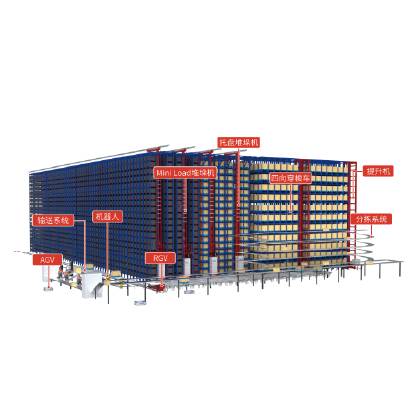
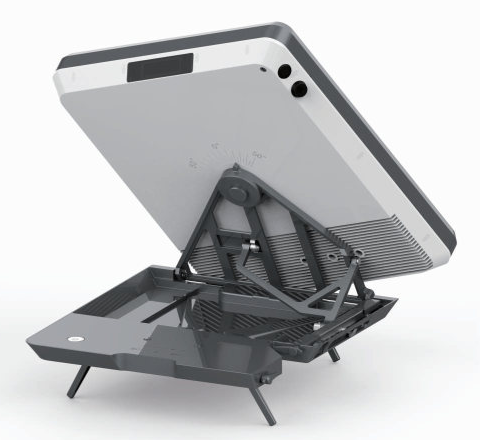
Flat Portable Satellite Terminal 0.35m Aperture Manual Portable Terminal
China Starwin Science & Technology Co., Ltd.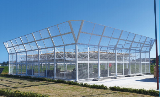
TWP16 P-Band Tropospheric Wind Profile Radar
China Huayun Meteorological Technology Group Co., Ltd.
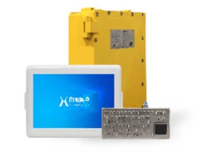
KJD127(A) Mining Explosion-Proof and Intrinsically Safe Computer
Taiyuan Xiangming Intelligent Control Technology Co., Ltd.
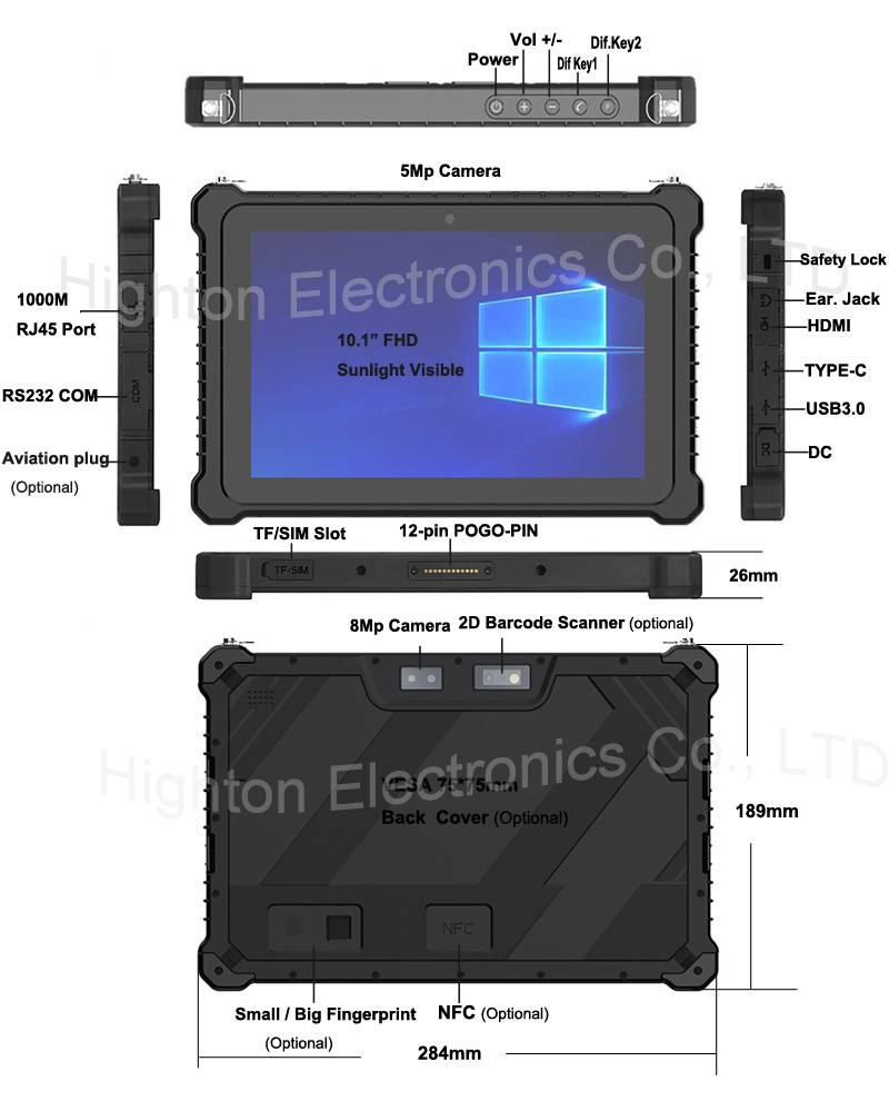
Hot Selling 10 Inch Intel N5100 I5 I7 FHD 8 +128GB 16+256GB Win10 Pro Win11 Pro 4G 5G Rugged Tablet PC Pad with NFC Barcode
Highton Electronics Co., Ltd.
20 Inch 1600*900 Full HD 60Hz TFT LED Monitor with VGA and DP Interfaces for Desktop Computers-Business Use
Guangzhou Zanying Optoelectronics Technology Co., Ltd.