

A team of materials scientists at Rice University in the United States has published research in the journal ACS Applied Electronic Materials, successfully developing a new method to directly grow two-dimensional semiconductor tungsten diselenide (WSe₂) on patterned gold electrodes. This approach uses chemical vapor deposition (CVD) technology, eliminating the need for transferring fragile 2D thin films during the conventional fabrication process.
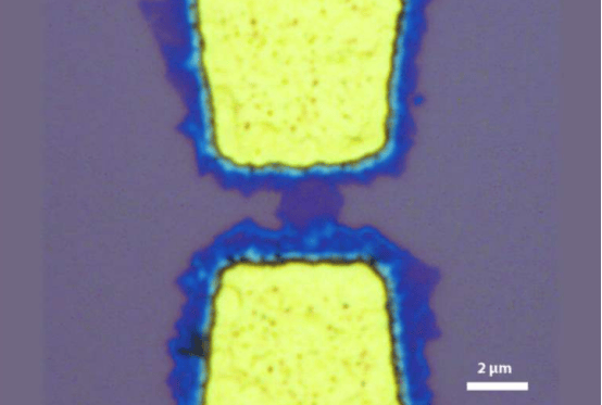
The research team demonstrated the feasibility of this transfer-free growth method by fabricating functional proof-of-concept transistors. Rice University PhD student Sathvik Ajay Iyengar stated: "This is the first demonstration of a transfer-free 2D device growth method, marking an important step toward lowering processing temperatures and achieving transfer-free integration processes for 2D semiconductors." The discovery originated from an unexpected observation during experiments: 2D materials preferentially form on gold surfaces during the chemical vapor deposition process.
Compared to traditional methods, this in-situ growth approach preserves material quality and enhances device performance. The team optimized precursor materials, reduced the synthesis temperature of the 2D semiconductor, and confirmed that it grows in a controlled, oriented manner. Rice University Professor of Materials Science and NanoEngineering Pulickel Ajayan noted: "Understanding the interaction mechanisms between 2D semiconductors and metals holds significant value for future device manufacturing and scalable production."
The research team used advanced imaging and chemical analysis techniques to verify the method's protective effect on the integrity of metal contacts. Co-first author Lucas Sassi emphasized: "The strong interaction between the metal and the 2D material during the growth process is the key to the success of this method. The lack of a reliable transfer-free growth approach has long been a major obstacle to the practical application of 2D semiconductors."
This method opens new pathways for applying atomically thin materials in next-generation transistors, solar cells, and other electronic technologies. The study also highlights the important role of international scientific collaboration in driving technological innovation; the project initially stemmed from discussions on 2D semiconductor manufacturing processes within a U.S.-India research initiative.