

Conventional photodetectors based on silicon semiconductors exhibit relatively low photoresponsivity, while two-dimensional semiconductor MoS₂ (molybdenum disulfide) is too thin, making it difficult to control its electrical properties through doping processes. These limitations have hindered the realization of high-performance photodetectors.
A research team at the Korea Advanced Institute of Science and Technology (KAIST) has overcome these technical barriers and developed the world's highest-performance self-powered photodetector, which can operate without external power in the presence of light. This breakthrough lays the foundation for battery-free, high-precision sensing in light-exposed environments for applications such as wearable devices, biosignal monitoring, Internet of Things (IoT) devices, autonomous vehicles, and robots.
The research team led by Professor Kayoung Lee from the School of Electrical Engineering developed a self-powered photodetector with sensitivity 20 times higher than existing products, achieving the highest performance level to date among similar technologies. The results were published in the journal Advanced Functional Materials.
The team introduced a "van der Waals bottom electrode," enabling the semiconductor to be extremely sensitive to electrical signals without doping, and fabricated a PN junction photodetector that can generate electrical signals by itself in the presence of light, even without an external power supply.
A PN junction is a structure formed by connecting p-type (hole-rich) and n-type (electron-rich) materials in a semiconductor. Under light illumination, this structure allows current to flow in one direction, making it a key component in photodetectors and solar cells.
Typically, creating a proper PN junction requires a process called doping, in which impurities are intentionally introduced into the semiconductor to alter its electrical characteristics. However, two-dimensional semiconductors like MoS₂ consist of only a few atomic layers, so traditional doping methods can easily damage the structure or degrade performance, making it difficult to form an ideal PN junction.
To overcome these limitations and maximize device performance, the research team designed a novel device structure that combines two key technologies: van der Waals electrodes and partial gating.
The partial gating structure applies electrical signals only to a portion of the two-dimensional semiconductor, controlling one side to behave as p-type and the other as n-type. This allows the device to function electrically like a PN junction without the need for doping.
In addition, considering that traditional metal electrodes form strong chemical bonds with the semiconductor, which can disrupt its lattice structure, the van der Waals bottom electrode adheres gently through van der Waals forces. This approach preserves the original structure of the two-dimensional semiconductor while ensuring effective electrical signal transmission.
This method ensures both structural stability and electrical performance, enabling the formation of a PN junction in thin two-dimensional semiconductors without damaging their structure.
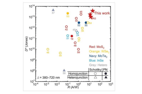
With this innovation, the team successfully realized a high-performance PN junction without doping. The device can generate electrical signals with extremely high sensitivity in the presence of light, even without an external power source. Its photodetection sensitivity (responsivity) exceeds 21A/W — more than 20 times higher than conventional powered sensors, 10 times higher than silicon-based self-powered sensors, and more than twice as high as existing MoS₂ sensors. Such high sensitivity means it can be immediately applied to high-precision sensors capable of detecting biosignals or operating in low-light environments.
Professor Kayoung Lee stated that they "achieved a sensitivity level unimaginable with silicon sensors. Although two-dimensional semiconductors are too thin for conventional doping processes, we successfully realized a PN junction that can control current without doping."
Professor Lee added: "This technology is not only applicable to sensors but can also be used in key components for controlling power inside smartphones and electronic devices, laying the foundation for miniaturization and self-powering in next-generation electronics."