

At the ITF World annual technology forum held in Antwerp on May 19, the Belgian microelectronics research center imec showcased for the first time a quantum dot qubit device manufactured using High Numerical Aperture Extreme Ultraviolet (High NA EUV) lithography. The device compresses the physical pitch between adjacent control electrodes to approximately 6 nanometers, and is considered by the industry as the first hardware device integrated using this advanced process, marking a critical leap for silicon-based quantum computing from laboratory prototypes to industrial-scale mass production in 300mm wafer fabs.
Quantum dot qubits store quantum information using the spin state of a single electron confined within a silicon nanostructure (i.e., the gate layer). Controlling these qubits requires precisely patterning multi-layer gate structures at the nanometer scale, where the electrode pitch between the plunger gate, responsible for quantum dot potential regulation, and the barrier gate directly determines the coupling strength between qubits and their immunity to interference. Kristiaan De Greve, imec researcher and Quantum Computing Program Director, stated bluntly in the announcement: "High NA EUV enables precise patterning of silicon quantum dot qubits. Since the coupling strength between adjacent quantum dots increases exponentially as their spacing decreases, we must reliably fabricate gaps of only a few nanometers between the qubit control electrodes. This is a true engineering feat, made possible by our integration and patterning teams and ASML's exceptional High NA EUV technology." The research was conducted in the joint imec-ASML High NA Lab in Veldhoven, the Netherlands.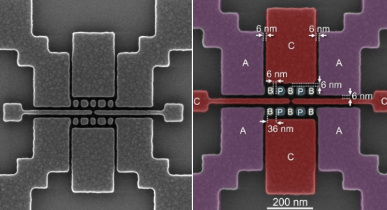
The core significance of achieving a 6nm pitch lies in fundamentally addressing the most challenging physical bottleneck in silicon qubit scalability. The coupling strength between quantum dots decays exponentially as the gap increases; if the gap cannot be compressed below 10 nanometers, the quantum dots cannot form sufficiently strong entanglement and logic operation capabilities. Simultaneously, qubits themselves are extremely sensitive to charge noise and interface defects—the larger the gate gap, the larger the quantum dot area exposed to the surrounding environment, making it more susceptible to interference from charge fluctuations and interface defect states, accelerating quantum decoherence and reducing qubit fidelity and operational success rates. Leveraging ASML's High NA EUV lithography system, the imec team utilized its 0.55 numerical aperture extreme ultraviolet light source to achieve resolution limits far exceeding traditional 193nm immersion lithography (0.33 NA), compressing the gap between the channel gate and barrier gate to 6 nanometers and successfully fabricating a functional qubit network. At this scale, it is theoretically possible to integrate millions of qubits on a single chip, meeting the basic engineering threshold for current practical-scale quantum computers.
imec's choice of silicon quantum dot spin qubits as its technical route offers the core advantage of high compatibility with existing CMOS chip manufacturing processes. Explaining the choice of this technical route, Sofie Beyne, imec Program Lead and Quantum Integration Engineer, pointed out: "We can leverage decades of accumulated semiconductor innovation and reuse the entire silicon manufacturing ecosystem, enabling quantum devices to leap from lab experiments to large-scale, manufacturable systems. This is precisely the significant advantage of silicon-based qubits." The gate stack structure of silicon-based quantum dot devices is highly similar to FinFET or Multi-Bridge Channel FETs in advanced logic chips in key process modules such as multi-layer metal interconnects, high-k dielectric deposition, and atomic layer etching, all of which can be completed using the mature process flows of existing 300mm wafer fabs. Compared to other quantum computing routes like superconducting or ion trap qubits, the silicon-based approach does not require building dedicated quantum computing foundries and can directly leverage the existing semiconductor supply chain for scaled verification, which is the fundamental reason it is referred to in the industry as an "industrial-grade qubit."
The technical highlights of this showcase are also reflected in the specific application flow of the High NA EUV lithography process in quantum device manufacturing. imec's integration and patterning team first grew high-quality silicon/silicon-germanium heterostructures on 300mm silicon wafers, followed by forming the initial layers of the gate stack through atomic layer deposition and chemical mechanical polishing. The High NA EUV lithography step is the core of the entire process: the 0.55 NA projection optical system focuses extreme ultraviolet light onto the photoresist, defining the 6nm-level electrode pitch in a single exposure, avoiding the overlay errors and line edge roughness that are difficult to control in traditional multi-patterning techniques. After exposure, the team used highly selective plasma etching to transfer the pattern into the metal gate material, completing the electrode interconnects through a subsequent damascene process. The entire process flow was completed in the standard cleanroom environment of a 300mm wafer fab, largely consistent with the manufacturing flow of advanced CMOS logic chips.
Previously, imec had already reproducibly achieved high-fidelity spin qubit operations on quantum dot structures through an optimized 300mm fab-compatible process flow, verifying the consistency of CMOS-compatible processes in qubit fabrication. With the introduction of High NA EUV lithography technology, the R&D focus has advanced from isolated laboratory prototypes to reproducible, standardized wafer manufacturing stages, proving that the most advanced lithography technology is equally applicable to the high-precision manufacturing of quantum devices. Headquartered in Leuven, Belgium, imec employs over 6,500 people and achieved revenue of 1.2 billion euros in 2025, holding a core position in the global semiconductor advanced process R&D field. High NA EUV lithography machines are widely considered a core technology supporting the development of advanced logic chips below 2 nanometers and high-density memories, and imec's demonstration indicates that this technology platform is also poised to become a key enabler for scaled quantum computing hardware. With the High NA EUV equipment in Leuven installed and ready, the research team has already begun preparations for the next phase of scaling towards industrial-grade levels.