

A research team from the Cockrell School of Engineering at the University of Texas at Austin has developed a desktop extreme ultraviolet (EUV) lithography device. Combined with volumetric 3D patterning technology, this innovation compresses semiconductor 3D nanostructure fabrication processes, which could previously take days, into just minutes of exposure. Aimed at the semiconductor research and development sector, this achievement seeks to lower the barrier to advanced lithography experiments, enabling more universities, laboratories, and materials teams to conduct chip manufacturing research.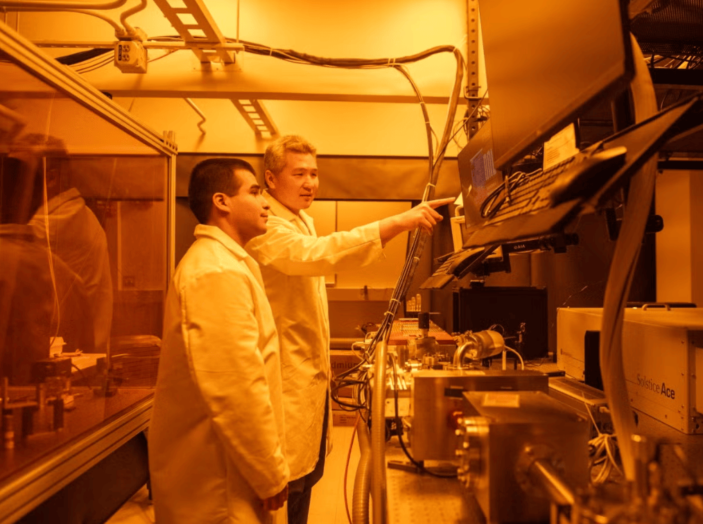
EUV lithography has long been one of the most technically challenging and cost-intensive steps in advanced chip manufacturing. Industrial-grade EUV lithography machines are typically large and complex, requiring coordinated operation of mirror optics, tin plasma light sources, masks, vacuum environments, and highly precise control systems. The cost of a single machine often reaches hundreds of millions of dollars, limiting the number of companies capable of commercial-scale manufacturing. The approach taken by the UT Austin team does not directly replicate wafer fab production-level equipment. Instead, they simplified the traditional EUV lithography system to its core components, creating a desktop device more suitable for scientific research. The accompanying volumetric 3D patterning method changes the pace of layer-by-layer 3D nanostructure fabrication: traditional commercial EUV lithography for 3D nanostructures requires sequential processing of 2D layers. While the actual exposure may not be lengthy, pre- and post-processing, alignment, and multi-layer fabrication extend the overall cycle. The new method processes multiple "layers" simultaneously in parallel, significantly shortening the experimental cycle for 3D nanopatterning. For research on new photoresists, memory structures, photonic devices, and semiconductor materials, this speed improvement directly impacts experimental iteration efficiency and helps diffuse EUV lithography research capabilities, previously concentrated in a few large institutions, to more research teams.
The research paper was published in *Nano Letters* under the title "Three-Dimensional Nanopatterning Using Extreme Ultraviolet Colloidal Talbot Lithography." The project is also related to the U.S. National Science Foundation's "Future of Semiconductors" program, and the research team has tested EUV materials co-designed by the University of Texas at Dallas and Johns Hopkins University.
The value of this achievement is concentrated in the semiconductor R&D sector, rather than immediately replacing wafer fab production equipment. At this stage, the process is primarily suitable for patterning periodic structures, making it more practically significant in experiments for memory chips, photonic devices, and nanomaterials. To enter more complex logic chip structures, improvements in pattern complexity, writing speed, material compatibility range, and processing consistency are needed. Nevertheless, the desktop EUV lithography device provides an important pathway: researchers can test EUV materials, 3D nanopatterns, and novel device structures at lower cost and within shorter cycles, reducing reliance on a few large lithography facilities. As AI chips, high-bandwidth memory, silicon photonics, quantum computing, and advanced packaging create greater demands for micro/nanostructures, tools capable of rapidly fabricating and validating 3D nanopatterns will become crucial infrastructure in semiconductor R&D and new material synthesis. The research team also noted that beyond chip manufacturing, the ability to pattern 3D nanostructures could be applied to areas such as nanomedicine, quantum computing, and new material synthesis, indicating that the potential application boundaries of this device extend beyond traditional integrated circuit manufacturing.
Future variables focus on the process's application scope and engineering scalability. For desktop EUV lithography to move from a research tool to broader applications, issues such as complex pattern writing, material system expansion, device stability, and repeatable processing precision must be addressed. For the semiconductor industry, this technology represents a democratization of advanced manufacturing R&D tools rather than a replacement for production lithography equipment. Its practical significance lies in shortening experimental cycles, reducing trial-and-error costs, and opening more entry points for EUV lithography and 3D nanopatterning research.