

The deposition precision of metal thin films directly determines the performance ceiling of devices. However, the low resistivity, high uniformity, and mass production-friendly process for molybdenum (Mo) thin films have long been industry challenges.
Recently, the Compound Semiconductor Pilot Line - Process Platform at JFS Laboratory collaborated deeply with atomic layer deposition (ALD) equipment manufacturers and achieved a new breakthrough in the ALD Mo process—using stable and efficient MoCl₂O₂ as a precursor, high-performance molybdenum thin films were prepared at 400°C. This marks the first development of this process on an 8-inch platform in China.
As a significant breakthrough in the fundamental technology field of compound semiconductors for the laboratory, this process meets mass production requirements in key indicators such as resistivity, uniformity, and step coverage. It plays a foundational supporting role in enhancing the performance of compound semiconductor devices, providing a viable model for the collaborative innovation of Chinese equipment and independent processes.

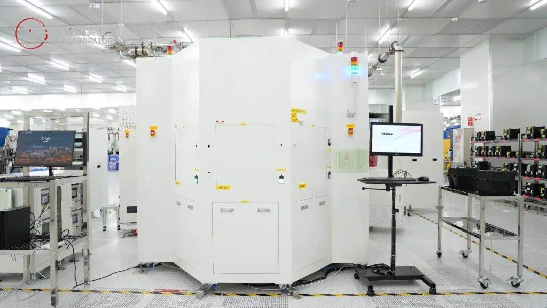
Engineers from the Process Platform's thin film team operating an ALD tool for process tuning and optimization
#1
Metal Mo: The Ideal Choice for Small-Scale Chips
As semiconductor device dimensions continue to shrink, traditional interconnect materials like tungsten (W) and copper (Cu) face challenges at the nanoscale, such as sharply increasing resistivity and electromigration failure. Molybdenum (Mo), with its excellent electrical properties and high-temperature stability, has emerged as an ideal alternative. At the nanoscale, the resistivity increase of Mo is far lower than that of tungsten (W) and copper (Cu), and it can be applied to both interconnect layers and gates, adapting to advanced manufacturing processes.
However, the process window for high-performance ALD Mo thin films is narrow and difficult to control. Balancing resistivity, uniformity, and step coverage in large-scale mass production has been a key focus of semiconductor industry research.
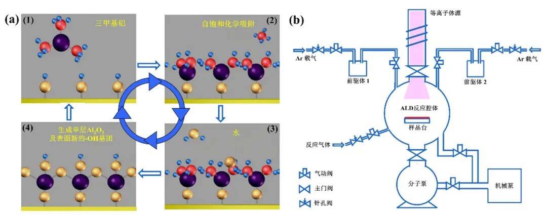
(a) Schematic diagram of the ALD working principle: using trimethylaluminum and water to prepare Al₂O₃ thin films as an example; (b) Simplified schematic diagram of an ALD system
#2
Fluorine-Free Precursor Eliminates Reliability Risks at the Source
The key to the process path breakthrough adopted by the JFS Laboratory Compound Semiconductor Pilot Line lies in the selection of precursors and reactants.
Traditional solutions often use fluorine-containing precursors, where fluorine residues can pose device reliability risks. This process solution uses MoCl₂O₂ as the precursor, which is completely fluorine-free, avoiding this problem at the source. Additionally, its high vapor pressure characteristic enables stable, high-throughput delivery, meeting mass production requirements.
Regarding reactants, hydrogen (H₂) plasma is used to replace traditional high-temperature processes. Its high reactivity allows for efficient deposition at a temperature of 400°C, avoiding high-temperature damage to the substrate. This ensures film quality while maintaining device compatibility.
Furthermore, this process eliminates the traditional step of preparing a molybdenum nitride (MoN) seed layer, allowing for the direct deposition of metallic Mo thin films, reducing process steps, shortening cycle times, and lowering costs.
In the early stages of process development, the team faced challenges such as unstable precursor delivery and low deposition rates. Through continuous technical攻关 and joint equipment-process tuning, the team overcame a series of technical challenges one by one, ultimately successfully achieving a stable and controllable mass production process.
#3
Independently Developed Process Synergizes with Chinese Equipment for Autonomous and Controllable Mass Production
In addition to the advantages of the independently developed process, the core highlight of this process suite lies in its collaborative development based on Chinese equipment. Process parameters were precisely optimized targeting the core characteristics of Chinese ALD equipment, such as the reaction chamber structure and gas delivery system.
This two-way adaptation brings benefits in two aspects: on one hand, it leverages the precise control advantages of Chinese equipment to achieve atomic-level uniform deposition; on the other hand, process optimization feeds back into the equipment, enhancing its operational performance. The process is stable and controllable, directly meeting the mass production needs of the industry, realizing a virtuous cycle where "Chinese equipment empowers the process, and the process feeds back into the equipment."
JFS Laboratory's Chinese equipment for ALD Mo
#4
Five Core Indicators Directly Target Industry Requirements
Through systematic testing, the ALD Mo thin film developed by the JFS Laboratory Compound Semiconductor Pilot Line demonstrates outstanding performance across five dimensions.
-
Low Resistivity: Controlled within 9 μΩ·cm, close to the intrinsic resistivity of bulk Mo material, far superior to traditional processes (typically >15 μΩ·cm). This can reduce device RC delay (resistance-capacitance delay), increase transmission speed, and reduce power consumption.
-
Good Uniformity: Within-wafer uniformity (1sigma) is 2%, and wafer-to-wafer uniformity is as low as 0.334%, ensuring consistent thin film performance across large-area wafers, providing a guarantee for mass production yield.
-
Excellent Step Coverage: Leveraging the conformality advantage of ALD, it can perfectly cover complex three-dimensional chip structures, adapting to manufacturing scenarios such as 3D NAND and high-end logic chips.
-
Dense Film Structure with No Obvious Defects: Can block impurity diffusion, enhance oxidation and corrosion resistance, reduce leakage risks, and extend device lifespan.
-
Simplified Process: Eliminates the need for a MoN seed layer, allowing direct deposition of Mo thin films, reducing process steps, shortening cycle times, and lowering material and equipment costs.
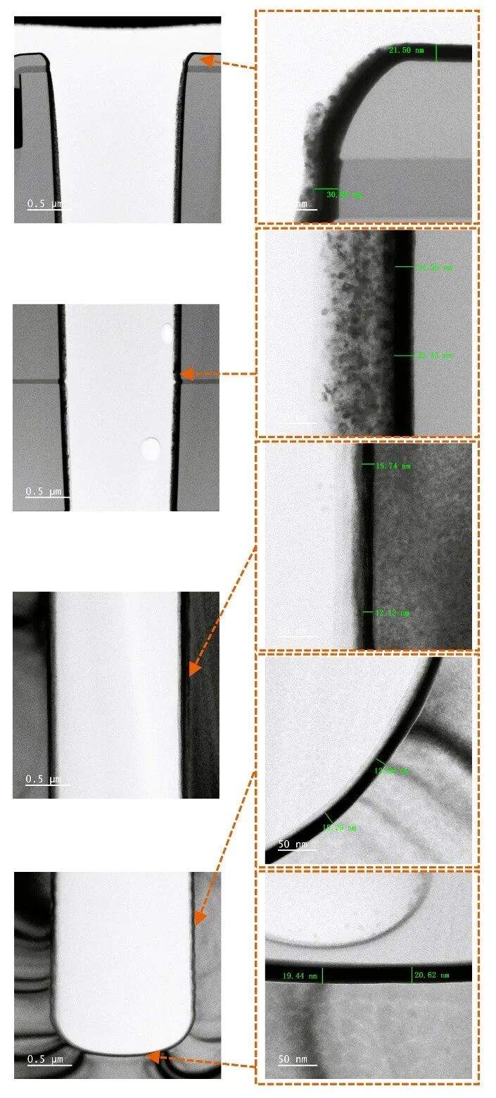
ALD Mo exhibits good step coverage in high aspect ratio structures (AR > 12:1)
The successful development of this process marks the first time China has achieved the development of an ALD Mo process on an 8-inch platform, with key indicators meeting mass production requirements. In 3D NAND manufacturing, the high step coverage can perfectly adapt to vertical channel structures, helping to increase storage capacity and read/write speeds. In logic chips at 7nm and below, the low resistivity directly results in lower RC delay, increasing computing speed and reducing power consumption. In DRAM (Dynamic Random Access Memory) manufacturing, the high uniformity and dense structure contribute to improved device stability and lifespan.
The successful breakthrough of this process also validates a judgment: The deep synergy between Chinese production equipment and independent processes can indeed deliver a high-level answer.