

With the large-scale deployment of 5G and the forward-looking exploration of 6G technology, the Internet of Things (IoT), ultra-high-speed sensing, and intelligent communication systems have placed unprecedented demands on the operating speed of transistors, requiring their cutoff frequency to surpass the critical threshold of 1 terahertz (THz). However, the performance of traditional high-frequency transistors, such as high-electron-mobility transistors (HEMTs) and heterojunction bipolar transistors (HBTs), is limited by the transit time of carriers in the channel or the base region of the bulk material, making it difficult to meet the application requirements of the terahertz frequency band. In recent years, vertical two-dimensional base transistors, which use two-dimensional materials such as graphene as the base, have significantly shortened the vertical transit time of carriers due to their atomic-level thickness, showing great potential for constructing terahertz transistors. Nevertheless, the prevalent issues of quantum tunneling barriers and interface defects in such devices cause severe carrier scattering, thereby limiting their current gain and high-frequency performance. Therefore, overcoming the interface bottleneck through novel modulation mechanisms to achieve high gain and enhance the cutoff frequency has become a core scientific challenge in the development of vertical two-dimensional base transistors.
To address this challenge, the Institute of Metal Research, Chinese Academy of Sciences, in collaboration with multiple research institutions, has proposed an innovative high-frequency device architecture—the silicon-graphene-germanium barristor. The related research results, titled "A high-frequency silicon-graphene-germanium barristor," were recently published in Nature Communications, marking a significant breakthrough in the research of high-frequency vertical two-dimensional base transistors.
This is the world's first barristor to successfully achieve radio frequency testing functionality. The research team first epitaxially grew wafer-scale single-crystal monolayer graphene on a germanium substrate via chemical vapor deposition, and then precisely stacked a single-crystal silicon film on top of the graphene to construct a high-quality silicon-graphene-germanium vertical heterostructure (as shown in Figure 1). This structure utilizes the asymmetric Schottky barriers formed at the interfaces between graphene and silicon, as well as graphene and germanium, combined with the quantum capacitance effect of graphene for work function modulation. This causes the current variation at the germanium terminal to be significantly larger than that at the silicon terminal, resulting in a common-emitter current gain as high as 1.8 ✖ 107, the highest record among reported transistors to date (as shown in Figure 2). In terms of high-frequency performance, the transistor achieves an intrinsic cutoff frequency (fT) of 132 GHz, surpassing the previous record for all vertical two-dimensional base transistors (as shown in Figure 3). Further device modeling and simulation analysis indicate that by optimizing material doping concentration, reducing contact resistance, and minimizing parasitic effects, the theoretical operating frequency of this device could potentially exceed 1 THz, entering the terahertz application band (as shown in Figure 4).
This research not only lays a solid foundation for the application of barristors in the fields of radio frequency and terahertz communication but also provides a novel technological pathway for ultra-high-speed signal processing in future IoT and 6G sensing systems.
This research work was led by Professor Sun Dongming and Professor Liu Chi from the Institute of Metal Research, Chinese Academy of Sciences, and was completed in collaboration with the team of Xue Zhongying from the Shanghai Institute of Microsystem and Information Technology, the team of Gao Jianjun from East China Normal University, the team of Wang Lingfei from the Institute of Microelectronics, and Professor Song Xubo from the National Key Laboratory of Solid-State Microwave Devices and Circuits. Wang Xiaoyue and Qiao Zishen from the Institute of Metal Research, Chinese Academy of Sciences, and Sun Shaotang from the Institute of Microelectronics are the co-first authors of the paper. This research was supported by the National Natural Science Foundation of China, the National Key Research and Development Program, the Liaoning Provincial Outstanding Youth Fund Program, and other funding sources.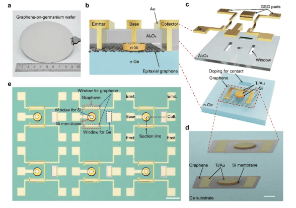 Figure 1. Device structure of the high-frequency silicon-graphene-germanium transistor. a. Epitaxial graphene wafer; b. Cross-sectional schematic of the device; c. Exploded view of the device structure; d. Scanning electron microscope image; e. Optical image of the device array.
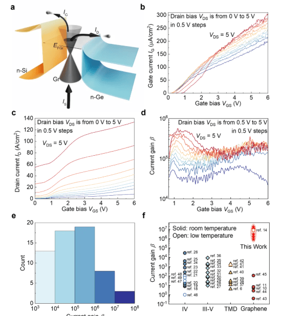
Figure 2. Barristor mechanism and DC characteristics. a. Asymmetric Schottky barrier energy band diagram; b. Device input characteristics; c. Device transfer characteristics; d. Current gain as a function of gate voltage; e. Statistical analysis of device gain; f. Benchmarking of gain against transistors from other material systems.
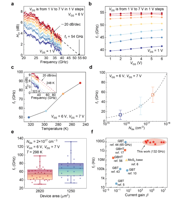
Figure 3. Radio frequency characteristics of the barristor. a. Gain H21 frequency characteristics under different bias voltages; b. Relationship between current gain cutoff frequency and bias voltage; c. Temperature dependence of the cutoff frequency; d. Cutoff frequency distribution at different germanium doping concentrations; e. Statistics of cutoff frequency for different device areas; f. Benchmarking of radio frequency performance against other vertical two-dimensional base transistors.
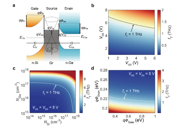
Figure 4. Compact physical model of the silicon-graphene-germanium barristor. a. Capacitance model and energy band schematic; b. Cutoff frequency as a function of bias voltage; c. Cutoff frequency as a function of doping concentration; d. Cutoff frequency as a function of Schottky barrier height.
This achievement demonstrates that Chinese research teams are advancing towards engineering-level testing in the direction of high-frequency devices based on two-dimensional materials. Graphene-based devices have long faced the transformation challenge of "strong material performance, difficult device integration." This study validates wafer-scale single-crystal graphene, heterojunction interface quality, and radio frequency indicators within the same system, providing a clearer experimental foundation for the subsequent exploration of terahertz electronic devices.