
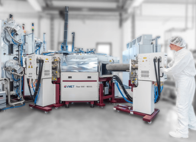
On July 30, the first Star600-EOSS 12-inch high-end precision optical magnetron sputtering mass-production equipment, independently developed by Jiangsu Xiantao Microelectronics, completed equipment assembly and joint commissioning at the production base in Xuzhou High-tech Zone, Jiangsu Province. It successfully passed automation and process verification and was officially delivered to a leading domestic wafer foundry. The smooth shipment of this first equipment marks a significant breakthrough for the company in the high-end wafer-level optical coating equipment field, from R&D and manufacturing to industrialized delivery, further advancing the localization of this equipment.
Global Advanced Wafer-Level Optical Coating Technology Achieves Localization in China
The Star600-EOSS is a high-end wafer-level precision optical magnetron sputtering equipment developed based on the Group's existing technical capabilities. Leveraging the Group's core patents, process database, and complete machine design system, Jiangsu Xiantao successfully achieved the engineering implementation of internationally advanced technology, and completed process adaptation and optimization through its own R&D capabilities, providing robust equipment support for high-end optical thin film manufacturing.
Multiple Core Technical Advantages to Meet High-Precision Manufacturing Needs for 12-Inch Wafers
The Star600-EOSS is specifically designed for 12-inch wafer-level optical coating and offers multiple advantages around the core process requirements of thin film deposition. The equipment adopts a twin rotating cathode sputter-up structure design, which physically reduces particle generation and enhances process stability. It supports full 12-inch wafer processing, with intra-wafer film thickness uniformity of ≤±0.3% and inter-wafer process stability within 0.3%, making it perfectly suitable for mass production of precision optical thin films such as IR-cut filters, AR anti-reflective coatings, optical waveguide dielectric films, and narrowband filters with over 100 layers, delivering excellent product performance with no wavelength shift and stable yield. In addition, the equipment integrates an in-situ broadband spectroscopic online monitoring system for real-time closed-loop correction of deposited film thickness. In terms of automation, it comes standard with an EFEM front-end module, is compatible with industry-standard 12-inch FOUP wafer cassettes, and achieves fully automatic cassette-to-cassette transfer via a vacuum-adsorption robot, while supporting SECS/GEM interconnection with factory MES systems for 7×24-hour unattended continuous production. The equipment features a modular process design, is equipped with multi-station independent magnetron cathode units, allows free switching between multiple target materials, and offers optional ion sources, in-situ plasma pretreatment, and low-temperature temperature control platforms, balancing the dual requirements of R&D sample preparation flexibility and large-scale mass production stability.
Building an Integrated Solution Capability with Synergy Between Materials and Equipment
Unlike single equipment manufacturers, Jiangsu Xiantao leverages the complete industrial chain advantages of its parent company, Xiantao Technology Group, to establish a vertically integrated core competitiveness spanning "high-purity target materials—complete coating equipment—thin film process development." In the field of optical thin film applications, the company combines the Group's high-purity indium, tantalum, titanium, silicon, and other optical target material resources to simultaneously complete target material matching and process recipe development based on customer product requirements, providing customers with one-stop customized coating solutions. The successful shipment of this equipment is a significant achievement in the company's continued efforts to advance independent R&D and industrial application of core equipment. In the future, the company will continue to focus on innovation in advanced thin film deposition technology, further contributing to the high-quality development of precision optics, wafer-level optics, and the semiconductor industry.