SK hynix Advances Construction of KRW 874.6 Billion Semiconductor Test Facility
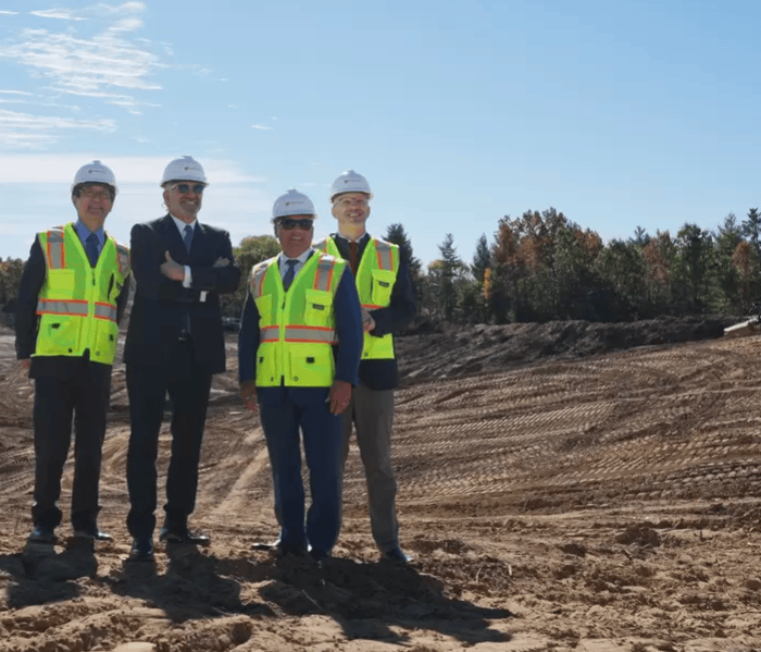
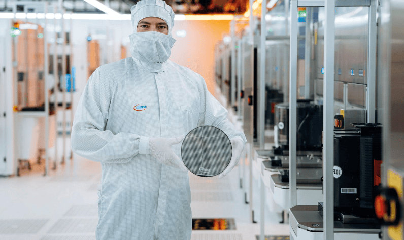
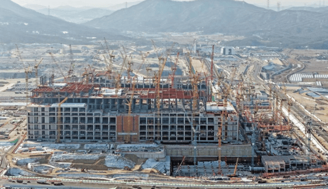
en.Wedoany.com Reported - On November 11, the Trinity Fab test facility for semiconductor materials, components, and equipment suppliers entered the final interior finishing stage inside the first wafer fab of the Yongin Semiconductor Cluster in Gyeonggi Province, South Korea. The project involves a total investment of KRW 874.6 billion, jointly funded by SK hynix, the South Korean central government, and local governments, and is scheduled to open in May 2027. The facility is located on the third floor of the first wafer fab and plans to build approximately 3,305 square meters of cleanroom space, providing suppliers with a process validation environment that closely mirrors actual chip mass-production conditions.
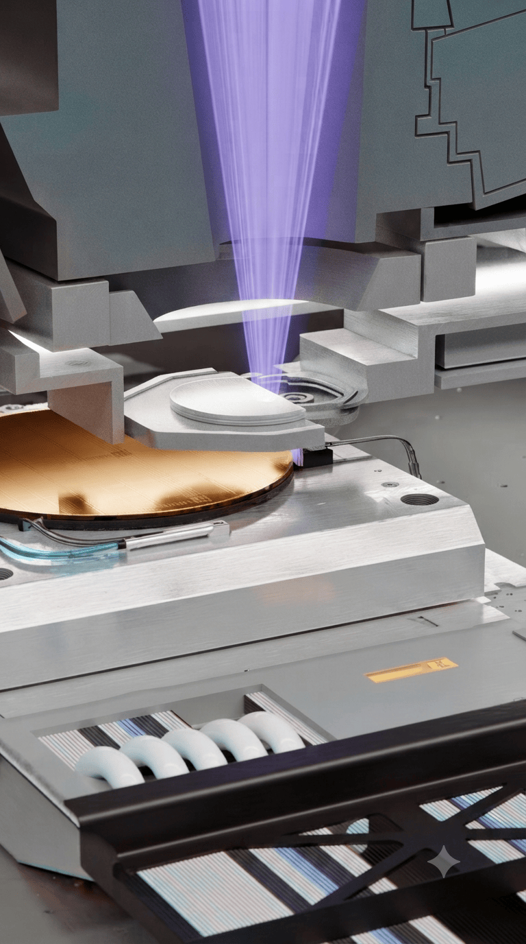
Of the project funding, SK hynix bears KRW 443.2 billion, the South Korean central government bears KRW 373.6 billion, and the Gyeonggi Province and Yongin City local governments bear KRW 57.7 billion. The facility will rely on a 12-inch wafer test platform, covering semiconductor manufacturing processes including photolithography, etching, deposition, cleaning, and inspection, providing a shared process environment for materials, components, and equipment companies to conduct product validation.
The facility is planned to be equipped with 51 semiconductor front-end process and inspection tools, plus 4 computer systems, totaling 55 units of equipment and systems. The cleanroom will also include 15 equipment rental test areas for suppliers to install and test their independently developed equipment. The first batch of 37 tools is scheduled to be installed by October 2027.
Trinity Fab is located inside the first wafer fab in Yongin, adjacent to SK hynix's own memory chip production cleanrooms, but uses independent access channels and security systems. The project will be operated by an independent non-profit organization, and participating companies can conduct material performance evaluation, process equipment validation, and mass-production compatibility testing within the facility.
SK hynix previously proposed on July 2 to invest KRW 1.4 trillion over the next five years to support semiconductor suppliers, with support covering four stages: R&D, validation, mass production, and sales. The R&D support mechanism allows eligible suppliers to receive advance payment of up to 50% of initial development costs, and provides agreed-upon cost compensation for projects that do not meet development targets.
Related Products

TWP16 P-Band Tropospheric Wind Profile Radar
China Huayun Meteorological Technology Group Co., Ltd.
JiuTian OneSky Pilot—Intelligent Management And Service Platform
China Times Prospect Science & Technology Co., Ltd.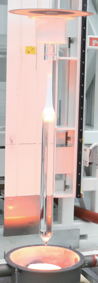
G.652.D Wavelength-extended Non-dispersion Shifted Single-mode Optical Fiber
HONGAN GROUP CO., LTD.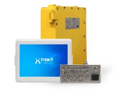
KJD127(A) Mining Explosion-Proof and Intrinsically Safe Computer
Taiyuan Xiangming Intelligent Control Technology Co., Ltd.
GYTA Type Non-Self-Supporting Aerial/Duct Optical Cable
TONGDING INTERCONNECTION INFORMATION CO., LTD.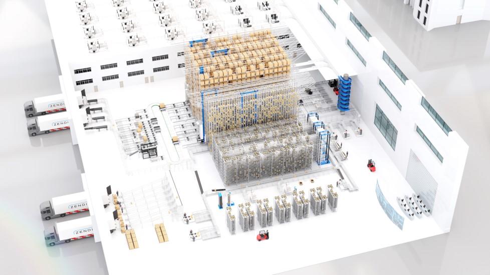
One-Stop Steward Service for the Entire Logistics System Integration Chain
Zhongding Intelligent (Wuxi) Technology Co., Ltd.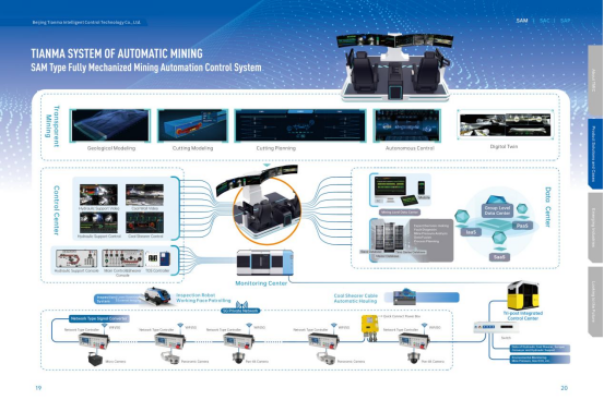
Comprehensive Mining Automation Control System
Beijing Tianma Intelligent Control Technology Co., Ltd.