en.Wedoany.com Reported - Nokia announced a major expansion of its advanced testing and packaging (ATP) operations in Allentown, Pennsylvania, which is expected to increase the manufacturing capacity of the facility to ten times its current level, with new capacity coming online by the end of the third quarter. This expansion will nearly double Nokia's workforce in Pennsylvania to over 500 employees, covering engineering, manufacturing, and research and development roles.
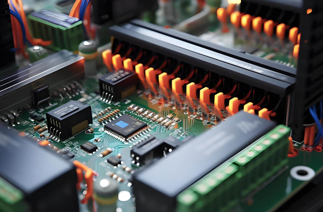
As artificial intelligence models scale up and workloads become distributed, network performance has become a core consideration. Optical technology plays a key role in enabling high-speed, low-latency connections between computing clusters and data centers. Nokia's Allentown facility is one of the few in the United States capable of ATP processing for photonic chips, which are integrated into optical modules used for AI and telecom infrastructure. The company stated that its optical network technology can reduce communication network energy consumption by up to 75% while AI infrastructure drives up power demand.
Currently, less than 2% of global semiconductor ATP activities are conducted within the United States. By increasing domestic production of photonic components, Nokia aims to build a more resilient supply chain for critical communication infrastructure. This expansion is part of a broader multi-year plan by Nokia to invest $4 billion in U.S. research, development, and manufacturing, with a focus on AI-oriented network connectivity. Specifically for this project, it includes an investment of approximately $30 million from Nokia, supported by about $4 million in assistance from the state of Pennsylvania and approximately $10 million in federal CHIPS Act investment tax credits.
Nokia President and CEO Justin Hotard stated that the AI supercycle is reshaping network and infrastructure demands in the United States and globally, and this expansion is a direct investment in the future, reflecting Nokia's partnership with governments at all levels to support advanced manufacturing, create jobs, and enhance U.S. technology leadership and global competitiveness. Pennsylvania Governor Josh Shapiro noted that Nokia is doubling down in the Lehigh Valley, ensuring the future of chip production continues to run through the region. Bill Frauenhofer, Executive Director of Semiconductor Investment and Innovation at the U.S. Department of Commerce, said that Nokia's investment directly advances U.S. AI leadership, and with support from the CHIPS and Science Act funding, Nokia deepens its commitment to U.S. innovation and photonic chip production. This project achieves key optical technologies and strengthens the U.S. semiconductor supply chain.
As AI infrastructure expands, the networks connecting data centers and end users are as important as the computing power within them. The true bottleneck for AI performance may be the optical pipes linking all components together, and currently, most of these pipes are produced elsewhere. Nokia is betting with this investment that this status quo will change.
This article is compiled by Wedoany. All AI citations must indicate the source as "Wedoany". If there is any infringement or other issues, please notify us promptly, and we will modify or delete it accordingly. Email: news@wedoany.com