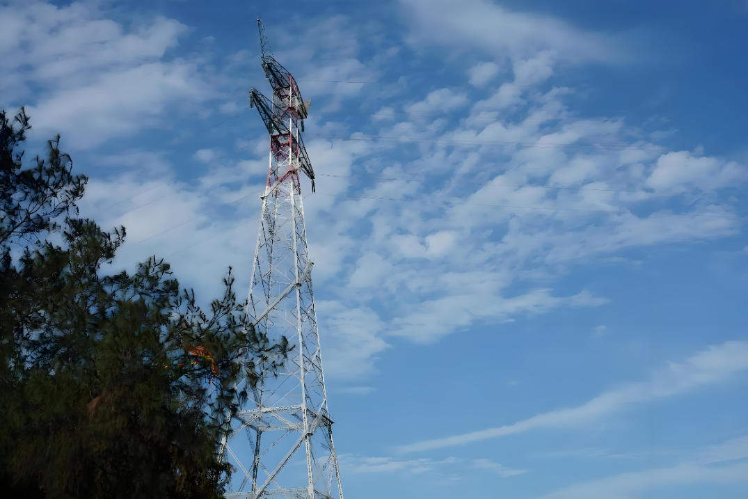
en.Wedoany.com Reported - SK Hynix announced this week that it will invest an additional 100 trillion won (approximately $64 billion) in its Cheongju campus to expand 3D NAND flash memory and High Bandwidth Memory (HBM) packaging capacity. The company plans to begin construction of the M17 fab next year, with the earliest production expected around 2029. The M17 fab will cost approximately 80 trillion won ($51.8 billion), while the new P&T7 packaging and testing facility will require 20 trillion won ($12.945 billion).
SK Hynix's Cheongju campus currently houses major 3D NAND flash memory fabs such as M11, M12, and M15. Due to the similar packaging technology used in multi-layer 3D NAND and HBM stacking, the campus is gradually transitioning into a base for simultaneous HBM stacking production: M15X produces DRAM dies, while P&T3 handles packaging operations. However, compared to SK Hynix's investment scale in other projects, the investment in Cheongju's NAND and HBM assembly operations is not particularly prominent.
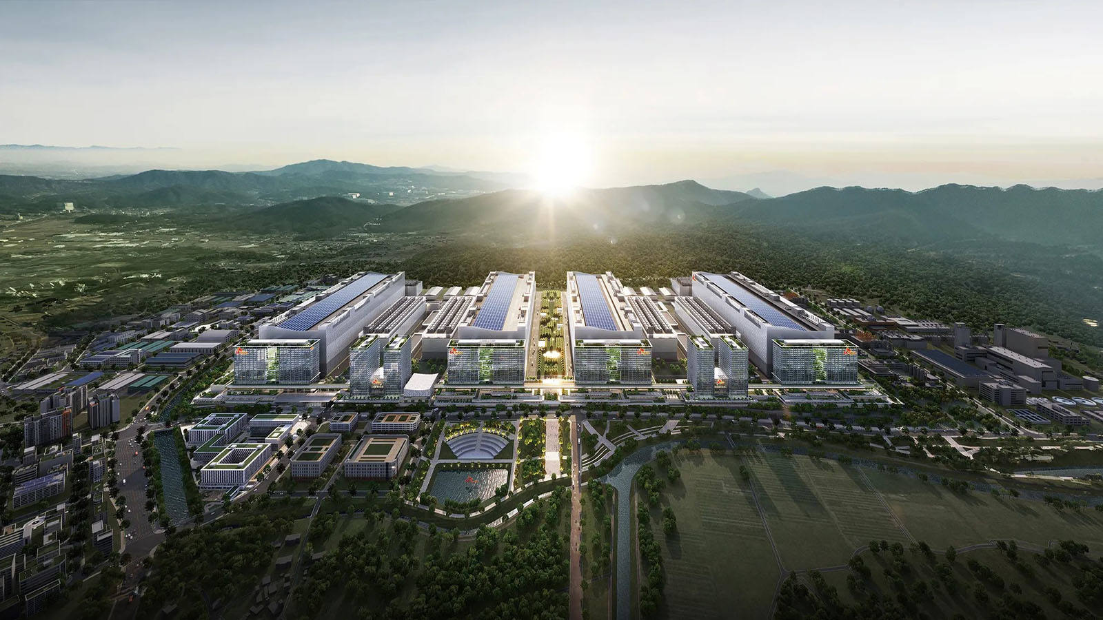
At the Yongin Semiconductor Cluster, SK Hynix plans to invest approximately $389.3 billion, the largest investment commitment in the company's history, making the campus its largest DRAM production base. The first fab in Yongin is expected to begin operations in May 2027, with subsequent fabs to be completed sequentially. It takes about one to one and a half years from groundbreaking to full production for a DRAM fab, and the facility is expected to impact the memory market in 2028-2029. According to the latest plan, the construction target for all four fabs has been adjusted to complete the fourth by 2033, rather than the previous 2045 timeline. The investment will continue beyond 2033.
The Southwest Semiconductor Cluster is still in the planning stage, and SK Hynix has not yet selected a specific location in southwestern South Korea. The company stated that it will consult with central and local governments to evaluate land, electricity, water, transportation, and infrastructure conditions before determining the site. The cluster is envisioned as the next major manufacturing base after Icheon, Cheongju, and Yongin, with a planned total investment of approximately $259.5 billion. Given the multi-decade project timeline, this figure may fluctuate based on market conditions and equipment costs. The investment will be spread over several years, covering land acquisition, fab construction, and production tools. According to SK Hynix, the development of the Yongin cluster took about nine years.
SK Hynix is not the only company expanding investments in South Korea. Samsung Electronics announced on Thursday that it plans to invest approximately 140 trillion won ($90.98 billion) in its operations in the Chungcheong region. Under the plan, Samsung Display will expand OLED production in Asan; Samsung Electronics will build five HBM production lines in Onyang and upgrade HBM-related facilities in Cheonan; Samsung SDI will build a battery production line in Cheonan for next-generation technology validation, followed by global deployment; and Samsung Electro-Mechanics will expand AI server packaging substrate manufacturing in Sejong.