Applied Materials Unveils $5 Billion Semiconductor R&D Center in the United States
en.Wedoany.com Reported - On October 12, Applied Materials officially unveiled the Equipment and Process Innovation and Commercialization Center (EPIC Center) in Sunnyvale, California, USA. The center plans to invest approximately $5 billion gradually as customer R&D projects are launched, building a collaborative R&D facility for next-generation semiconductor materials, manufacturing equipment, and process technologies. TSMC, Intel, SK hynix, Micron, and Samsung Electronics are founding partners.
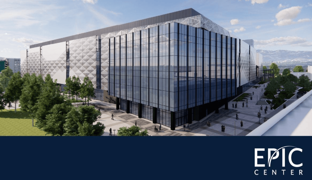
The EPIC Center has a floor area of approximately 600,000 square feet (about 55,700 square meters), and houses an advanced cleanroom of nearly 4 acres (about 16,200 square meters). Cumulative investment in facility construction exceeded 6 million work hours, and the cleanroom roof uses 34 large trusses, each with a span of nearly 300 feet (about 91 meters). Applied Materials positions the facility as the world's largest collaborative R&D center for semiconductor process technology and manufacturing equipment.
The center integrates semiconductor materials research, equipment development, process integration, and manufacturing validation into a single R&D facility, adopting a parallel development approach in which chipmakers and Applied Materials engineering teams jointly optimize materials, equipment, and manufacturing processes. The related R&D targets leading logic processes, three-dimensional transistor structures, advanced interconnects, memory, and advanced packaging technologies, and covers technology validation from early-stage R&D to large-scale manufacturing introduction.
Companies participating in the EPIC Center also include innovation partners Broadcom, Advantest, SCREEN, KIOXIA, and Besi. Research partners include Arizona State University, Rensselaer Polytechnic Institute, Stanford University, UC Berkeley, and the UCLA Samueli School of Engineering. Each partner will arrange for R&D personnel to participate in joint projects according to its own technology roadmap.
Under the announced collaboration arrangements, TSMC will focus on research into next-generation logic device materials, three-dimensional transistors, and interconnect processes; SK hynix will conduct joint R&D around HBM, DRAM, and NAND memory technologies; Samsung Electronics will participate in the development of advanced logic processes, future memory architectures, and three-dimensional integration technologies. The center will subsequently gradually expand capital investment and the scope of collaboration as customer R&D projects advance.
Related Products


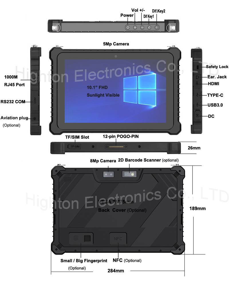
Hot Selling 10 Inch Intel N5100 I5 I7 FHD 8 +128GB 16+256GB Win10 Pro Win11 Pro 4G 5G Rugged Tablet PC Pad with NFC Barcode
Highton Electronics Co., Ltd.
20 Inch 1600*900 Full HD 60Hz TFT LED Monitor with VGA and DP Interfaces for Desktop Computers-Business Use
Guangzhou Zanying Optoelectronics Technology Co., Ltd.
G.652.D Wavelength-extended Non-dispersion Shifted Single-mode Optical Fiber
HONGAN GROUP CO., LTD.

MUX Series Communication Interface Device for Security and Stability Control System
Nanjing NR Electric Co., Ltd.

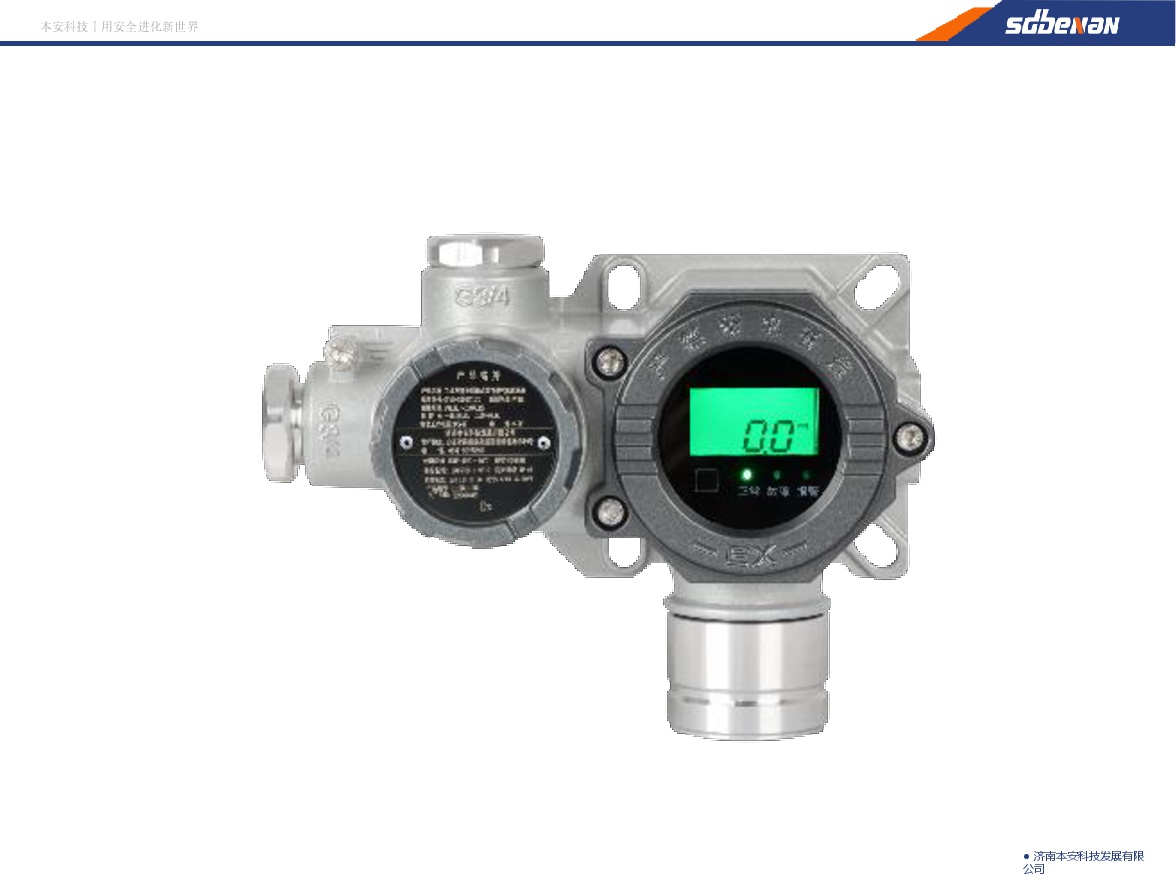
Industrial and Commercial Point-Type Gas Detector
Jinan Benan Technology Development Co., Ltd.