en.Wedoany.com Reported - Researchers at the Massachusetts Institute of Technology (MIT) have used a new technique called "implosion fabrication" to create nanophotonic devices that can be used for visible light manipulation applications such as optical computing. The related paper was recently published in Nature Photonics.
The technique allows researchers to use light patterning to imprint features on a hydrogel with a resolution of about 800 nanometers, and then shrink these features down to less than 100 nanometers. Because the resolution is smaller than the wavelength of visible light (380 to 750 nanometers), the nanophotonic devices can bend light in specific ways to perform optical computing. Throughout the process, the hydrogel shrinks more than tenfold in each dimension, resulting in a volume reduction of about 2,000 times.
"To achieve nanophotonics applications in visible light, we need to fabricate nanostructures with feature size resolutions of less than 100 nanometers," said Quansan Yang, one of the lead authors, a former MIT postdoc and current assistant professor at the University of Washington. "Only then can we precisely create structures that manipulate visible light." Co-first author Gaojie Yang, also a former MIT postdoc, is another lead author. Senior authors include Professor Peter So, director of MIT's Laser Biomedical Research Center, and Professor Edward Boyden, a professor of neurotechnology. Boyden is also a Howard Hughes Medical Institute investigator and a member of several MIT institutes.
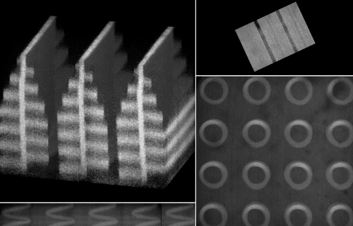
During the fabrication process, the hydrogel is first immersed in a photosensitive dye. A laser then excites the photosensitizer at specific locations to generate free radicals, which break chemical bonds to form voids. Afterwards, the hydrogel undergoes ionic solution soaking and supercritical drying, ultimately shrinking in volume by a factor of 2,000. The researchers used this technique to create various 3D shapes such as helices and butterfly wing structures, and fabricated a device capable of performing digital classification tasks. This device introduces light diffraction through void patterns, mimicking a neural network to complete digit recognition.
"This is a purely optical system that can effectively perform optical computing," said So. "You can manipulate material properties at every tiny location," added Dushan Wadduwage, one of the paper's authors, a former MIT postdoc and current assistant professor at Old Dominion University. "We have millions of locations where properties need to be decided, which becomes a design problem that can be solved using deep learning algorithms to design new components." The researchers currently plan to use the same principle to build optical devices that can classify cells flowing through microfluidic devices, aiming to identify circulating tumor cells in blood samples. This method could also be used for high-throughput imaging analysis of biopsy tissue samples, or adapted for other materials to fabricate channels for 3D nanofluidic devices. The research was funded in part by the MIT-Fujikura Collaboration Fund, the U.S. Army Research Office, Lisa Yang and Y. Eva Tan, John Doerr, the Open Philanthropy Project, the Howard Hughes Medical Institute, and the National Institutes of Health.
This article is compiled by Wedoany. All AI citations must indicate the source as "Wedoany". If there is any infringement or other issues, please notify us promptly, and we will modify or delete it accordingly. Email: news@wedoany.com