en.Wedoany.com Reported - This solution can eliminate the troublesome optical 3D mask effect, improve lithography resolution, and manufacture smaller chips at lower cost.
From data centers supporting next-generation artificial intelligence, to critical medical devices, automobiles, and mobile devices or computers, semiconductor-based chips are indispensable core components of modern life.
As technology iterates and power demands continue to rise, researchers are dedicated to developing smaller chips, which requires precise circuit design at the single-nanometer scale. Technologies such as extreme ultraviolet (EUV) lithography have opened new pathways for miniaturized chips, but this technology faces significant physical, engineering, and cost challenges that limit its current implementation and mass production.
Professor Tsumoru Shintake from the Okinawa Institute of Science and Technology Graduate University (OIST) published a study in the Journal of Micro/Nanopatterning, Materials, and Metrology, proposing a disruptive redesign of the illumination system and projection optics used in high numerical aperture (high-NA) EUV lithography. Simulation results show that this solution can eliminate the troublesome optical 3D mask effect, improve lithography resolution, and manufacture smaller chips at lower cost compared to existing EUV processes.
Tsumoru Shintake stated: "Currently, a single EUV lithography machine costs hundreds of millions of euros. My new solution can achieve fine pattern fabrication at the 2–3 nanometer scale at a cost far lower than the most advanced commercial models available today."
He elaborated on the downstream application value of miniature semiconductor chips against the backdrop of growing demand from the AI industry. "The International Energy Agency predicts that, driven by high-energy-consumption applications such as intelligent agents, data center electricity consumption will double by 2030. Chips manufactured using high-NA lithography processes have higher device integration density and shorter circuit signal transmission distances, which can minimize energy loss and reduce the power cost per operation."
Tsumoru Shintake added, "These high-density chips also generate less heat, reducing the energy required for accompanying cooling. This technological improvement is expected to significantly lower the overall power load of data centers."
What is EUV Lithography? A Primer on Semiconductor Chip Formation Principles
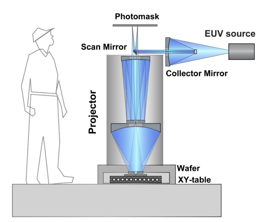
EUV lithography technology generates extreme ultraviolet light with a wavelength of only 13.5 nanometers. The light beam is directed into an illumination system and then shines onto a reflective photomask, which carries the complete circuit pattern template. The reflected patterned beam passes through a projection lens, which uses multiple sets of mirrors to reduce and focus the pattern onto the surface of a silicon wafer. Subsequent processes then etch the circuit pattern onto the wafer.
To achieve higher integration circuit fabrication, the industry has begun tackling high-NA EUV lithography technology. Numerical aperture (NA) determines the angular range over which an optical system can accept or emit light; the higher the NA, the larger the angle of light that can be captured, allowing the lens to resolve finer patterns. Theoretically, lithography resolution (the smallest distinguishable feature size) is inversely proportional to NA, and a higher NA enables finer pattern formation on chips.
In the early days of EUV lithography research in the 1990s, researchers explored high-NA coaxial optical architectures similar to Tsumoru Shintake's approach, where the mask, projection lens, and wafer remain coaxially aligned. This coaxial structure is simple, but researchers at the time were unable to resolve the pattern distortion, blurring, and various optical errors that worsened as NA increased.
To overcome these challenges, Tsumoru Shintake initially attempted to use a set of concave and convex mirrors as the projection lens. After iterative optimization, he ultimately developed a two-stage optical structure, with each stage paired with concave and convex mirror sets.
Initial simulation results were not ideal. He then discovered that precisely arranged multiple mirror groups, through multiple reflections, could cancel out various optical aberrations while maintaining high-NA performance. After months of extensive calculations using the optical simulation software OpTaliX, he determined the ideal curvature and placement of the mirrors to achieve high NA while ensuring imaging quality.

Toward Scalable Semiconductor Mass Production
Like all research projects, this solution still has certain limitations: the simulation assumes mirrors with 100% reflectivity and no defects, and transitioning from the simulation model to a physical device will require extensive specialized engineering optimization. Building a physical prototype is the team's next core task. The research group has already initiated EUV hardware development, aiming to create a low-cost, high-performance EUV lithography machine.
Tsumoru Shintake concluded: "This solution can significantly simplify the structure of high-NA equipment, reduce manufacturing costs, and open up new development space for semiconductor manufacturing. We have the capability to develop lithography machines costing only one-quarter of current commercial equipment. Leveraging higher-precision lithography processes, we can fabricate memory chips with higher integration density and logic chips with better energy efficiency. This technology could bring transformative social value, supporting data centers and the next generation of AI development, making various electronic products faster and more energy-efficient, with the potential for lower long-term usage costs."
This article is compiled by Wedoany. All AI citations must indicate the source as "Wedoany". If there is any infringement or other issues, please notify us promptly, and we will modify or delete it accordingly. Email: news@wedoany.com