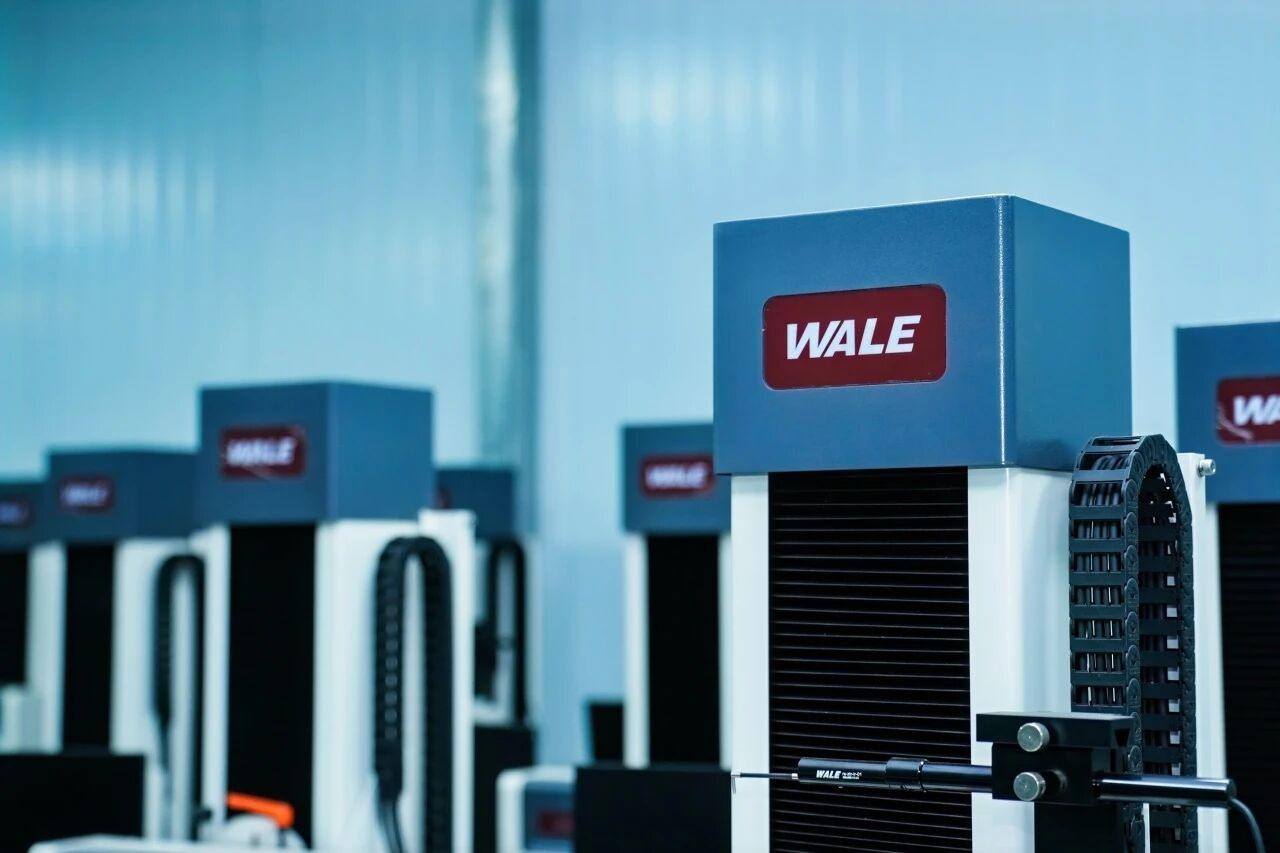
en.Wedoany.com Reported - Teledyne DALSA, a subsidiary of Teledyne Technologies Canada, announced in June 2026 the launch of the Linea HS2 8k TDI (Time Delay Integration) high-speed imaging camera, expanding the Linea HS2 series from the original 16k resolution to 8k resolution. The camera features a backside-illuminated (BSI) CMOS TDI sensor with a pixel size of 5 µm and a maximum line rate of 1 MHz, targeting high-speed inspection applications such as semiconductor wafer inspection, high-density interconnect (HDI), and genomics flow cells.
Headquartered in Waterloo, Ontario, Canada, Teledyne DALSA is a digital imaging company under Teledyne Technologies Incorporated (NYSE: TDY), specializing in the design, manufacture, and sale of high-performance charge-coupled device (CCD) and complementary metal-oxide-semiconductor (CMOS) image sensors and cameras. Its products are widely used in industrial inspection, life sciences, medical imaging, and defense. TDI technology enhances image signals by moving charge across multiple integration stages to match object motion, making it particularly suitable for high-speed, low-light line scan imaging applications.
According to Teledyne DALSA, the Linea HS2 8k model, together with the existing 16k model, forms a complete Linea HS2 series product portfolio. The series sensors adopt a multi-array charge domain architecture, supporting flexible configuration for image quality, line rate, dynamic range, or full well capacity to meet different inspection application needs. On-chip binning helps maintain throughput at higher web speeds, and the camera is equipped with a Camera Link HS CX4 connector for active optical cables, offering electromagnetic interference immunity.
The newly launched Linea HS2 8k model fills a gap in the series for medium-resolution high-speed inspection applications, complementing the 16k model. For inspection scenarios that do not require the ultra-high resolution of 16k, the 8k model provides a more cost-effective option while retaining the high-speed performance and image quality of the Linea HS2 series. In semiconductor wafer inspection, high-speed high-resolution line scan cameras can detect micro-defects on wafer surfaces; in high-density interconnect inspection, they can check line width, line spacing, and hole position accuracy of printed circuit boards; and in genomics flow cell inspection, they enable high-speed scanning for fluorescence imaging.
This article is compiled by Wedoany. All AI citations must indicate the source as "Wedoany". If there is any infringement or other issues, please notify us promptly, and we will modify or delete it accordingly. Email: news@wedoany.com