en.Wedoany.com Reported - Qualcomm announced its entry into data center AI infrastructure, disclosing the AI250 series accelerator based on near-memory computing architecture at its 2026 Investor Day last week. The technology stacks DRAM to form unified compute and storage modules, aiming to deliver superior inference efficiency compared to current GPUs.
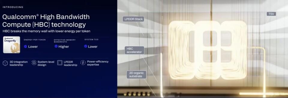
Qualcomm has named the technology High Bandwidth Compute (HBC). Tony Pialis, Executive Vice President of Data Center, stated during the investor presentation that HBC offers the performance advantages of SRAM while combining the density and storage capacity of HBM stacks. The AI250 series is planned for launch next year as part of the Dragonfly rack system, marking a significant shift in Qualcomm's AI infrastructure strategy. Although Snapdragon processors already integrate NPUs, Qualcomm has struggled to gain market attention comparable to Nvidia, AMD, or even startups like Cerebras in the data center space.
Compared to the GPUs of the two giants, Qualcomm's AI series accelerators currently lack an advantage, but the company is seeking to make its mark in the data center. The AI250 single card claims 768 GB of storage capacity and up to 133 TB/s of effective memory bandwidth. For reference, Nvidia's Groq 3 LPU offers only 500 MB of SRAM and 150 TB/s of bandwidth. Qualcomm acknowledges that these figures rely on the term "effective," as its AI200-based Dragonfly system claims a total "effective" memory bandwidth of 414 TB/s across all 56 chips, but achieving this with only 8800 MT/s LPDDR5x would require a 6720-bit wide bus, which the company almost certainly does not have. Qualcomm insists this represents "the pure physical bandwidth of the LPDDR interface" but declines to explain how it achieves what Nvidia requires eight HBM3e stacks to accomplish.
Qualcomm's marketing materials indicate that with the shift to HBC, the AI250 will deliver 18 times the effective bandwidth of the AI200, and the upcoming AI300 will offer 54 times the bandwidth. These "effective" multipliers are actually characteristics of the HBC architecture. By moving some XPU compute units beneath the DRAM, chip power consumption can be significantly reduced. Traditional data center GPUs rely on data exchange between HBM and compute dies, and even with advanced packaging technologies like TSMC's CoWoS, power consumption remains substantial. In contrast, HBC stacks DRAM directly on top of some logic, using through-silicon vias (TSVs) for connections, drastically shortening the path from compute to memory. Pialis likened this to working in the building where you live, requiring only vertical movement without needing highways and expensive silicon interposers.
The benefit of performing bandwidth-limited operations on the base die is that it reduces the amount of data transferred between HBC and the SoC, thereby amplifying memory bandwidth. Qualcomm may not run the entire AI software stack on HBC, as higher memory bandwidth primarily benefits the decoding phase, where all active weights of the model flow out of memory token by token in an autoregressive manner. Decoding is not compute-intensive, so performing it partially or entirely in HBC avoids the thermal constraints of burying compute units under multiple layers of DRAM. Qualcomm stated that the AI250 can be used as a standalone AI accelerator or in a disaggregated inference architecture, using GPUs or other Qualcomm components for prompt processing while the AI250 accelerates memory-intensive decoding operations. Qualcomm did not provide peak FLOPS data in the AI250 disclosure and declined to share details upon request.
Although Qualcomm is one of the earlier chip design companies to hype near-memory or HBC, the technology is not out of reach for Nvidia or AMD. Nvidia and AMD are reportedly collaborating with HBM suppliers and TSMC to develop custom base dies to enhance next-generation chip performance. Qualcomm stated that its HBC "uses LPDDR memory in a purpose-built near-memory computing architecture that combines compute and highly accelerated memory bandwidth in a 3D stacked silicon design. HBC is a unique architecture designed to address the AI data movement bottleneck by bringing compute closer to memory, improving memory bandwidth efficiency and enhancing energy efficiency for AI inference workloads. HBM has more DRAM stacks, uses 2.5D interposers to route more lines, and does not perform compute in the base logic die." AI chip startup d-Matrix is also developing accelerators that use 3D stacked DRAM to scale memory compute capabilities.
During the Investor Day, Qualcomm also announced the acquisition of AI software startup Modular. Modular was founded by Tim Davis and Chris Lattner, the latter being the creator of LLVM, Clang, the Swift programming language, and the Multi-Level Intermediate Representation (MLIR) compiler infrastructure. At Modular, Lattner and the team developed Mojo, a low-level programming interface for GPUs that offers a high-performance alternative to Nvidia's CUDA or AMD's HIP and ROCm stacks. The core concept is that users should be able to write high-performance AI applications without worrying about the underlying hardware. For Qualcomm, Mojo provides an opportunity to bypass the CUDA moat, allowing customers to avoid choosing a single platform and instead develop applications that can run on any available compute resources. Modular also developed a service platform called Max, similar to SGLang or vLLM, which can run interchangeably on AMD or Nvidia hardware and, being built on Mojo, theoretically requires almost no manual tuning.
If the acquisition is completed this year without regulatory intervention, the product should help Qualcomm compete in an environment where software is becoming more important than hardware. Qualcomm plans to launch the AI200 series racks later this year, with the first HBC-based AI250 starting in 2027, and the second-generation HBC platform scheduled for 2028. The company has also previously disclosed details about its new data center CPU.