
en.Wedoany.com Reported - On July 1, the Belgian microelectronics research center (imec) officially released its 2026 edition of the semiconductor process technology roadmap. This roadmap, co-developed with global industry leaders including TSMC, Intel, NVIDIA, AMD, Samsung, and ASML, outlines the technological evolution direction for chip manufacturing over the next decade or more.
According to the roadmap, a 0.3nm (A3) class process technology could be achieved by 2038, with the vertical stacking architecture of complementary field-effect transistors (CFETs) serving as the core solution to overcome physical limits and sustain Moore's Law.
Traditional Scaling Nears Limits, CPP Stalls at A10 Node
The semiconductor industry has now entered the era of 2nm mass production, with a transistor gate contact pitch (CPP) of approximately 48nm. According to imec's plan, the A14-class process is expected to debut around 2028, with CPP shrinking to 45nm and standard cell height reducing to about 115nm. High-NA EUV lithography equipment will be introduced at this stage.
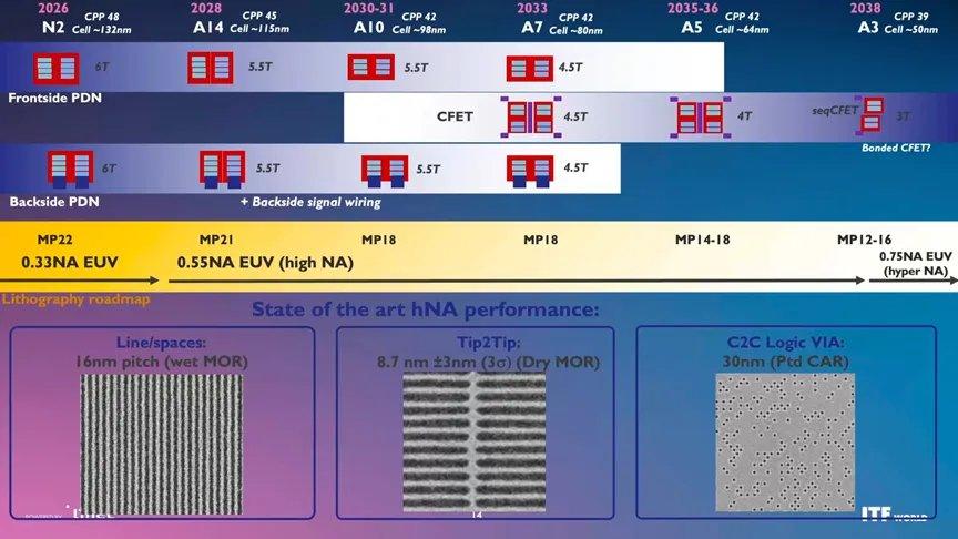
However, the true turning point arrives with the A10 node (1nm), expected between 2030 and 2031. After this, CPP will remain at 42nm for an extended period, with no further reduction. This means the traditional path of increasing chip density solely by shrinking transistor dimensions laterally will hit its physical limits around 2030.
Julien Ryckaert, Vice President of R&D at imec, noted: "Entering the A7 phase, which is the seventh angstrom-generation (fourth-generation nanosheet), we find that traditional nanosheet device technology faces increasing challenges in dimensional scaling."
CFET Vertical Stacking: Adding a Third Dimension to Transistor Scaling
Since lateral scaling has reached its end, imec's proposed solution is to move from two dimensions to three.
The key inflection point in the roadmap is expected in 2033—when the A7-class process (approximately 0.7nm) transitions to a CFET architecture. Unlike current FinFET and GAA transistors, which place n-type and p-type transistors side by side, CFET stacks them vertically, adding a third dimension to transistor scaling and enabling more efficient use of space.
imec's roadmap shows that while CPP for A7 remains at 42nm, CFET technology can reduce standard cell height from 98nm at A10 to approximately 80nm. Subsequently, A5 (2035-2036) will use a four-track library to further reduce cell height to about 64nm; by the A3 generation in 2038, CPP will shrink to 39nm, with cell height reaching 50nm.
To achieve the A3 node target, imec believes it may rely on ultra-high numerical aperture lithography technologies such as Hyper-NA EUV.
TSMC Already Deploying, CFET Competition Begins
As one of the co-developers of the imec roadmap, TSMC has already made moves in CFET technology. Reports indicate that TSMC showcased a CFET ring oscillator composed of approximately 1,000 transistors at its technology forum, leading the industry.
Currently, TSMC's most advanced process is 2nm, using first-generation nanosheet transistor technology. The subsequent A14 process is expected to debut in 2028, offering a 15% speed increase at the same power consumption or a 30% power reduction at the same speed compared to N2. The A13 and A12 processes, featuring super power rails, are planned for production in 2029.
From "Transistor Size" to "Standard Cell Area"
The most profound implication of imec's roadmap is its redefinition of Moore's Law. Future chip density improvements will no longer be measured by the size of individual transistors, but rather by the reduction in standard cell area (cell height × CPP).
From the 6-track cell of N2 to the 3-track cell of A3, standard cell height drops from approximately 132nm to about 50nm—a nearly threefold reduction. This means that even if CPP scaling stalls, designers can still achieve increased transistor density by lowering cell height.
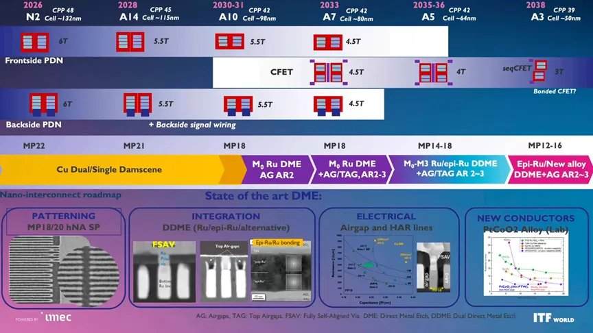
Power Delivery and Heat Dissipation Become New Bottlenecks
Given the trend of AI workloads becoming the primary driver of semiconductor demand, imec has proposed the concept of heterogeneous large-scale integration (HLSI). It envisions future systems highly integrating logic chips, memory, power delivery, optical I/O, and advanced 3D/2.5D packaging. To this end, imec has established a cross-technology co-optimization (XTCO) framework, aiming to break down technical barriers and achieve comprehensive optimization at the system level.
Ryckaert pointed out that as transistor vertical integration and multi-chip packaging become the norm, power delivery design and heat dissipation will become the most severe technical bottlenecks in the future. Emerging technologies, including backside power delivery networks (BSPDN) and integrated voltage regulators (IVR) within packages, must be co-optimized at the system level to continuously enhance chip computing density and energy efficiency without increasing power costs.
Summary:
imec's roadmap clearly demonstrates that while the traditional Moore's Law centered on "shrinking transistors" faces significant challenges, the logic density of semiconductors will maintain strong growth momentum over the next decade or more through a multi-pronged approach: reducing standard cell area, vertical integration via CFET, and system-level co-optimization. From 2nm nanosheets to 0.3nm CFETs, the semiconductor industry is undergoing a comprehensive transformation spanning materials, equipment, and architecture.