en.Wedoany.com Reported - A high-end advanced packaging and testing project with a total investment of 7.8 billion yuan has recently initiated engineering design bidding in Shanghai, entering the preparation phase for implementation. The project focuses on building high-end advanced packaging and testing production capacity, aiming to fill the gap in packaging and testing capacity for high-value-added sectors such as China's AI chips and automotive electronics, thereby supporting the high-end upgrade of Shanghai's integrated circuit industry.
The project covers a total land area of approximately 119,538 square meters, with a total construction area tentatively set at 225,698 square meters. The building facilities include production and R&D workshops, comprehensive office and dormitory buildings, power plants, multiple types of specialized warehouses, a 110kV substation, a corridor system, an underground garage, and park supporting facilities, meeting the mass production, R&D, and park operation needs of high-end packaging and testing production lines. The construction period is planned from 2026 to 2027. On July 3, a bidding announcement for the construction drawing design of the integrated circuit high-end manufacturing project was released, initiating the engineering design bidding to lay the foundation for subsequent civil construction, equipment installation, and production line setup.
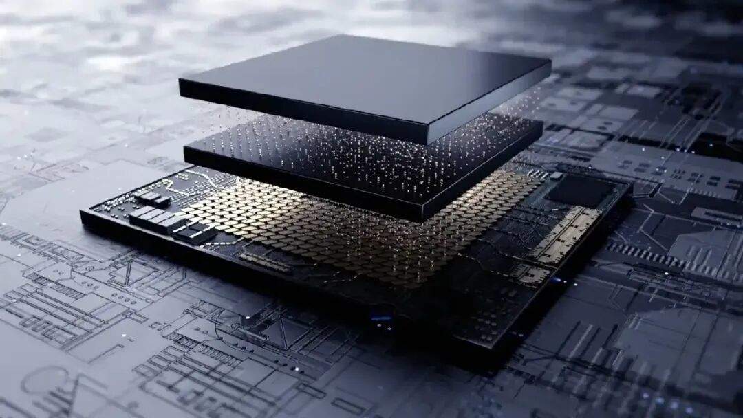
The project is primarily targeting the high-growth high-end chip packaging sector. Upon completion, it will focus on meeting the packaging and testing demands of AI computing chips, high-performance processors, and high-end automotive electronics, precisely addressing the capacity gaps caused by the AI computing boom and the upgrade of automotive chips. It aims to tackle the industry pain point of insufficient supply of high-end advanced packaging and testing capacity in China. In terms of technical layout, the project will concentrate on advancing cutting-edge packaging technologies such as 2.5D/3D wafer-level packaging, heterogeneous integration, and high-density system-in-package, strengthening mass production support capabilities, filling the gap in China's advanced packaging process mass production, promoting the large-scale implementation of high-end packaging and testing technologies, and narrowing the technology and capacity gap with top international packaging and testing manufacturers.
Industry insiders indicate that the landing of this 7.8 billion yuan high-end packaging and testing project in Shanghai is a key strategic move by China's packaging and testing leaders to increase investment in advanced processes and seize opportunities in the AI and automotive electronics industries. With the smooth progress, completion, and operation of the project, it will effectively expand China's high-end advanced packaging and testing capacity, improve the full-chain layout of Shanghai's integrated circuit industry, continuously enhance China's self-sufficiency in high-end chip packaging and testing, and inject new momentum into the high-quality development of the semiconductor industry.