Spanish Submer Approved to Build AI Data Center in India
en.Wedoany.com Reported - On July 13, Spanish digital infrastructure company Submer Group announced plans to advance a semiconductor and digital infrastructure project worth approximately $2 billion in the Indian state of Madhya Pradesh. The physical construction already confirmed is a data center project located in the Achhapura Industrial Area. After receiving the company's land application, the Madhya Pradesh government allocated 15 acres of industrial land within six days, moving the project from preliminary cooperation and site selection phases to concrete land allocation.
The announcement was made during the "Madhya Pradesh Technology Growth Summit 3.0: Global Capability Centers, Data Centers, and Semiconductors Conference." Submer's overall project is expected to create approximately 5,000 direct jobs, but the specific allocation of the $2 billion investment among data centers, semiconductor facilities, R&D centers, and supporting infrastructure has not yet been disclosed. Therefore, the entire amount cannot currently be interpreted as the construction cost of a single semiconductor wafer fab or a single data center.
Based on confirmed project progress, the 15-acre plot in the Achhapura Industrial Area will be used for the data center project. Subsequent construction typically requires advancing campus planning, architectural design, power connection, substation facilities, fiber optic networks, server room structures, cooling systems, and server equipment installation. Submer has not yet disclosed the data center's floor area on this plot, initial IT capacity, power supply scale, construction start date, or commissioning timeline. The project still requires more detailed engineering design and construction approvals.
This project is a continuation of the cooperation agreement previously signed between Spanish Submer and the Madhya Pradesh government. In July 2025, both parties announced plans to jointly develop up to 1 GW of liquid-cooled, AI-ready data center capacity, with construction directions including immersion liquid cooling, direct-to-chip cooling, and hybrid cooling systems. The facilities are primarily designed for high-density GPU servers and AI computing workloads, reducing the space and cooling energy consumption required by traditional air-cooling systems.
According to previously announced technical plans, in addition to participating in data center design and construction, Submer will also assist in developing liquid cooling facility design standards, establishing local supply chains, and conducting technical talent training. The Madhya Pradesh government is responsible for land, infrastructure connections, and related administrative support. The allocation of this 15-acre plot marks the first time this cooperation has resulted in a more defined project area, but whether this plot will host the initial phase of the 1 GW plan and how much computing capacity is planned for deployment remain to be confirmed in subsequent announcements.
High-density AI data centers have high requirements for external infrastructure. In addition to server rooms and cooling equipment, the project requires large-capacity substations, backup power supplies, high-speed internal networks within the data center, and multiple fiber optic connections to the operator's backbone network. If semiconductor-related facilities are built concurrently, additional specialized systems such as cleanrooms, specialty gases, ultrapure water, process exhaust, and precision environmental controls will be needed. However, current official announcements only specify the semiconductor industry investment commitment and data center land, without disclosing specific chip factory, packaging and testing production line, or semiconductor equipment installation plans.
The key milestones for the next phase of the project will be completing the master plan for the Achhapura plot, defining the initial data center capacity, finalizing power and fiber optic access plans, and commencing main construction. For the overall $2 billion project, further disclosure from Submer or the Madhya Pradesh government is needed regarding the construction timeline, phased scale, and specific engineering content corresponding to the semiconductor business.
Related Products
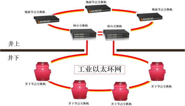

Mine Explosion-proof and Intrinsically Safe Industrial Ethernet Ring Network (10 Gigabit/Gigabit)
Chongqing Mas Sci&Tech Co., Ltd.
Conveyor Belt Intelligent Monitoring System
LUO YANG WIRE ROPE INSPECTION TECHNOLOGY CO., LTD.
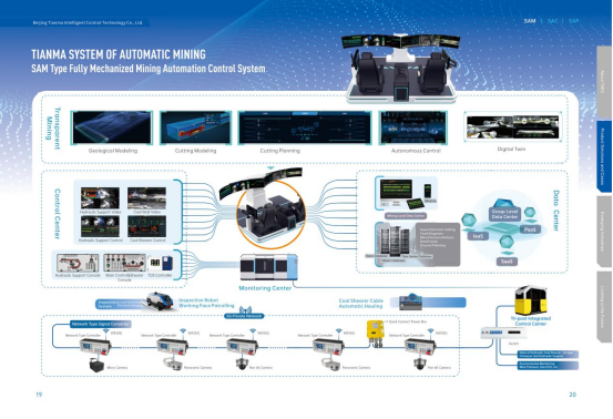
Comprehensive Mining Automation Control System
Beijing Tianma Intelligent Control Technology Co., Ltd.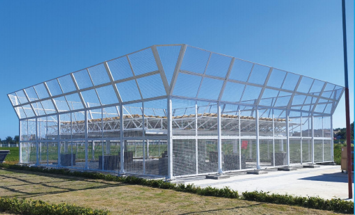
TWP16 P-Band Tropospheric Wind Profile Radar
China Huayun Meteorological Technology Group Co., Ltd.
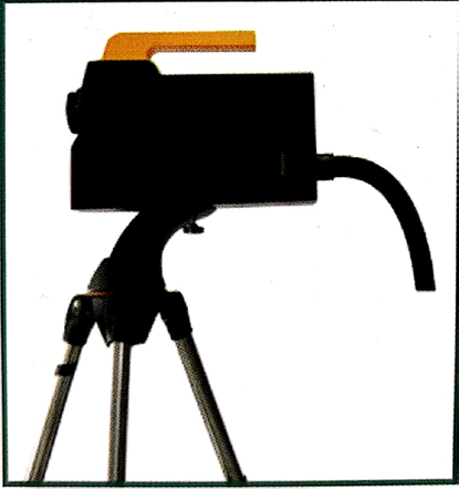
Automatic Aiming Laser Remote Obstacle Removal Robot
Pinggao Group Weihai High-Voltage Apparatus Co., Ltd.