Wedoany.com Report on Mar 11th, The semiconductor industry is at a critical turning point, as the traditional model of Moore's Law faces physical and economic limitations. The transition to 3D IC design has become central to technological evolution, driving changes in semiconductor design and integration methodologies. This necessitates a re-evaluation of design flows and enhanced industry collaboration.
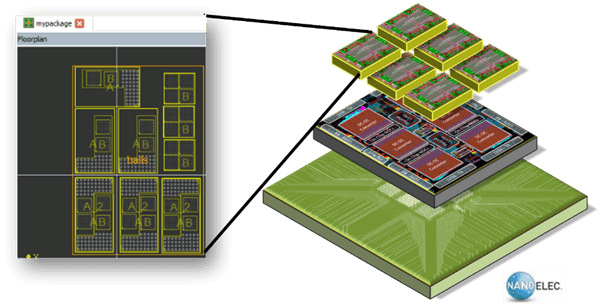
Figure 1. Arrayed tiles used for constructing chiplets.
3D IC technology is currently categorized mainly into 2.5D and true 3D integration. 2.5D technology places multiple chips side-by-side on a silicon interposer and is already widely used in high-performance computing. True 3D integration involves the direct stacking of chips, utilizing hybrid bonding technology to achieve high-density interconnects, offering performance advantages for applications like AI acceleration. Industry leaders such as hyperscale cloud providers are actively pushing the boundaries of 3D IC technology, but adoption across broader markets remains slower, with varying levels of design support.
Economic and technological factors drive 3D IC development. The cost of advanced process nodes is high, with non-recurring engineering expenses potentially exceeding $500 million, while 3D integration can reduce costs and improve yield. Technological drivers include the need for high-bandwidth, low-latency memory access. By placing memory closer to compute elements through 3D integration, the "memory wall" bottleneck can be alleviated. Traditional monolithic chip design is constrained by reticle size limits, and manufacturing large SoCs faces yield challenges. 3D IC technology offers a solution by integrating smaller, functionally optimized chiplets.

Figure 2. System technology co-optimization enables concurrent design work while improving the flow for each design segment.
High-bandwidth memory stacking has become a key component of 3D ICs. Modern designs often integrate multiple HBM stacks, with HBM4 expected to double the bandwidth of HBM3 by 2026. This underscores the importance of memory proximity and advanced packaging.
A successful transition to 3D IC requires a fundamental shift in design methodology and organizational structure. The traditional "over-the-wall" approach is no longer adequate, necessitating a system-centric flow that considers system-level issues like power delivery and thermal management early on. The industry faces new challenges, such as 3D verification and thermal modeling, requiring the development of new EDA tools. Siemens, through its technology portfolio including Calibre and Innovater3D IC, as well as partnerships and acquisitions, is facilitating the industry's evolution towards 3D IC integration.

Figure 3. Siemens' 3D IC thermal solution.
The future of 3D IC depends on the availability of a comprehensive EDA toolchain that supports the entire flow from architecture exploration to verification, integrating AI and machine learning. The industry is moving towards standardized chiplet integration, with standards like UCIe promoting an open market. Emerging technologies such as system-on-wafer and advanced organic substrates will expand the possibilities of 3D integration. While power delivery and thermal management remain challenges, continued R&D is expected to unlock the full potential of 3D IC technology.

Figure 4. Innovator3D IC solution suite cockpit.