en.Wedoany.com Reported - With the development of chip interconnection technology, circuit structures are becoming increasingly complex, and the threat of hidden defects to yield rates has significantly increased. How to detect issues such as short circuits and open circuits without damaging the circuit and address them precisely has become the primary task for improving device performance and yield in China's semiconductor integrated circuit field. Driven by this demand, laser technology has entered the public eye, leveraging its unique characteristics to open new paths for circuit inspection and repair.
Traditional electrical testing typically requires removing the insulating layer on the device surface or the electrodes of voltage-sensitive components to perform inspection operations on the underlying electrodes and circuit structures. Currently, the mainstream still relies on two traditional methods: mechanical window opening and chemical etching, which have long suffered from pain points such as significant damage, insufficient precision, and poor repair capability. Traditional window opening methods can easily damage the electrodes or brittle structures beneath devices that have suffered voltage breakdown, causing "false failures" that fail to reflect true performance. Meanwhile, traditional methods struggle to quantitatively control nanoscale residual oxides and cannot perform in-situ testing or localized repair for short circuits or open circuits, greatly affecting device uniformity and yield rates.
Chinese laser equipment company Huachuang Hongdu, leveraging its core light source advantages, has custom-developed targeted process solutions, forming a complete closed-loop system of "oxide layer removal—inspection—repair." In the laser lift-off process, femtosecond lasers, with their performance advantages of precise energy control, combined processing quality and efficiency, and no thermal accumulation effect, can achieve oxide layer removal with an area accuracy of ≤1μ㎡ and residual oxide volume of ≤1% without damaging the electrodes. After lift-off, electrical re-inspection confirms whether the electrode functions are normal and precisely locates fault points.
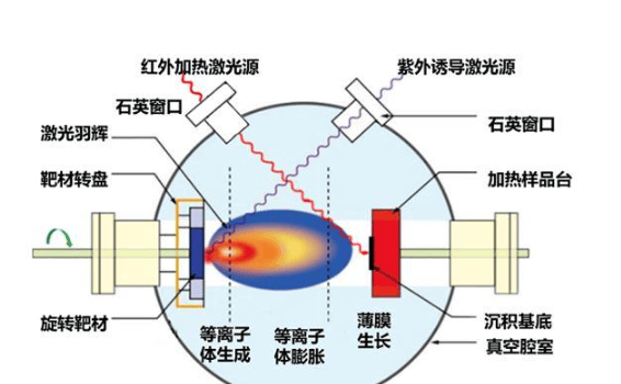
In the laser repair phase, for open circuit problems, laser-induced localized deposition thin-film technology can precisely "bridge" the break, restoring the electrical connection. The principle involves using high-energy ultraviolet pulsed lasers to bombard the target material, causing it to instantly vaporize and form a plasma plume. Substances within the plume, induced by the heating of an infrared laser, deposit on the defect site of the substrate and epitaxially grow into a thin film, achieving high-precision repair with a film repair area accuracy of ≤1μ㎡. For short circuit problems, femtosecond laser processing, with its high precision and cold processing characteristics, can vaporize and remove excess metal or conductive residues without damaging surrounding circuits, achieving a short circuit defect repair area accuracy of ≤±1μ㎡.
In the laser annealing phase, this technology employs localized precise heat treatment to reduce surface defects and impurities on the circuit, improve local structure and electrical performance, and accurately correct abnormal resistance values. Combined with high-stability lasers and two-color radiation thermometry, the annealing temperature stability is ≤±1℃, the annealing repair positioning accuracy is ≤±1μm, the single induction accuracy is ±5Ω, and the resistance value of the area to be repaired is increased by 10~50%. The three key processes mentioned above are deeply coupled with the inspection stages, forming a closed-loop workflow of "lift-off—inspection—repair—re-inspection," while also supporting the integration of fully automated loading and unloading modules to enhance yield and efficiency.
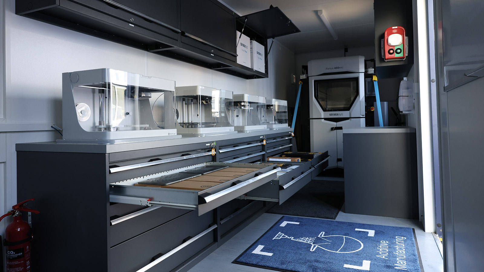
The stable realization of this laser processing solution fundamentally relies on the autonomous control of core light sources. Huachuang Hongdu focuses on high-reliability solid-state laser technology and has established a complete technical path from core light source R&D and mass production to laser application process testing for new scenarios and new materials.
This article is compiled by Wedoany. All AI citations must indicate the source as "Wedoany". If there is any infringement or other issues, please notify us promptly, and we will modify or delete it accordingly. Email: news@wedoany.com