en.Wedoany.com Reported - Recently, the Fourth-Generation Semiconductor Research Team and the New Technology Engineering Department of Shenzhen Pinghu Laboratory in China announced significant progress in both gallium oxide surface planarization and gold-free ohmic contact processes. Based on gallium oxide epitaxial wafers grown by metal-organic chemical vapor deposition (MOCVD), the team achieved a specific contact resistivity of 8E-7 Ω cm² using a gold-free process, while simultaneously developing a new surface planarization technique that reduces the root mean square (RMS) surface roughness of gallium oxide to 0.107 nm. Both core indicators have reached the industry's best levels, providing crucial support for the self-reliance and industrialization of China's fourth-generation semiconductors.
Gallium oxide is a core material in the global focus on ultra-wide bandgap semiconductors, offering outstanding advantages such as high voltage resistance, high temperature tolerance, and high power handling, making it an ideal choice for next-generation high-power electronic devices. However, two major technical bottlenecks have long hindered the mass production of gallium oxide devices: first, electrode contacts rely on the precious metal gold, leading to high costs and poor thermal stability; second, the rough surface of epitaxial wafers easily causes defects and electric field concentration, affecting device reliability. The research team at Shenzhen Pinghu Laboratory has now solved both industry challenges simultaneously.
Gold-Free Ohmic Contact Process: Eliminating Gold for Electrodes, Reducing Costs by 90% with Enhanced Stability
Gallium oxide ohmic contact engineering has long depended on gold (Au)-based systems, while gold-free ohmic contacts are a key technology for achieving mass production and industrial self-reliance. Although traditional gold-based contacts can reduce contact resistance to some extent, they suffer from critical bottlenecks such as high-temperature diffusion, poor thermal stability, high costs, and process incompatibility, directly limiting device performance and production feasibility.
By utilizing multi-layer stacking of non-precious metals and interface engineering, the team successfully achieved ohmic contacts with an excellent specific contact resistivity of 8E-7 Ω cm² (lower than the 1E-6 Ω·cm² of comparable gold-based processes). Compared to traditional gold-based processes, the new solution not only avoids process bottlenecks and pain points but also reduces electrode material costs by over 90%.
Gallium Oxide Surface Planarization Process: Transforming "Rough Sandpaper" into an "Atomic-Level Mirror"
Surface roughness is a key parameter for evaluating the quality of gallium oxide single-crystal substrates and homoepitaxial layers. Due to the significant morphological inheritance effect in gallium oxide epitaxial growth, surface undulations on the substrate are directly transferred to the epitaxial layer, further amplifying surface defects. A rough surface generates numerous lattice dangling bonds and interface defects, increasing interface state density, while surface micro-protrusions can cause localized electric field concentration, inducing premature device breakdown. To address this challenge, the research team developed a new surface planarization process that reduces the RMS surface roughness of epitaxial wafers to 0.107 nm—a reduction of over six times compared to the initial roughness—achieving atomic-level smoothness and significantly enhancing device stability and voltage resistance.
These breakthroughs in the two core processes directly bridge the critical link from gallium oxide materials to devices, significantly improving device performance and reliability. They lay a solid foundation for large-scale applications in high-power electronic fields such as new energy, urban rail transit, and smart grids, further consolidating China's independent innovation advantages in the ultra-wide bandgap semiconductor sector. In the future, as gold-free processes and ultra-smooth surface technologies continue to evolve, gallium oxide will move closer to large-scale commercial use, potentially entering industrial and civilian applications more quickly, driving China's fourth-generation semiconductor industry to a global leading position.
Notably, Shenzhen Pinghu Laboratory has been delivering frequent good news. The compound power semiconductor pilot platform, jointly established by the laboratory and Shenzhen Pengjin High-Tech Co., Ltd., was previously approved as a Guangdong Province Semiconductor and Integrated Circuit (Compound Power Semiconductor) Pilot Platform. This year, it has successively received recognition as a Shenzhen Compound Power Semiconductor Pilot Base and a Key Cultivation Pilot Platform by the Ministry of Industry and Information Technology. These two major designations mark a leapfrog upgrade from municipal support to provincial layout and national-level cultivation.
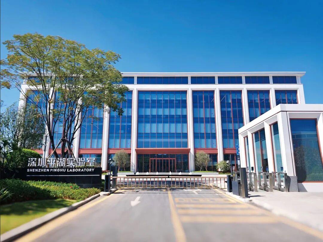
Shenzhen Pinghu Laboratory serves as the Shenzhen Comprehensive Platform of the National Third-Generation Semiconductor Technology Innovation Center and the Guangdong Province Semiconductor and Integrated Circuit (Compound Power Semiconductor) Pilot Platform, established by the Shenzhen Science and Technology Innovation Bureau. It focuses on core technology research in areas such as SiC, GaN, and next-generation advanced power electronic materials and devices, core equipment and components, and supporting material verification services.
The laboratory has built a fully functional modern park located in Luoshan Science and Technology Park, Longgang District, Shenzhen, covering an area of 130 mu. It boasts industry-leading wide bandgap power semiconductor R&D and production infrastructure, with over 380 sets of advanced international and domestic equipment and 9,500 square meters of Class 100 cleanroom space.
The laboratory brings together top R&D talents and experienced engineers from around the world, creating an open, public, and shared research center, pilot center, and analysis and testing center for the nation. It is committed to overcoming common challenges and key technologies in the third-generation semiconductor industry chain, continuously driving innovation, and completing the third-generation semiconductor industry chain. It aims to produce world-class innovations in next-generation semiconductors, cultivate world-class talent, and build an ecosystem with partners to jointly create a sustainable future.
This article is compiled by Wedoany. All AI citations must indicate the source as "Wedoany". If there is any infringement or other issues, please notify us promptly, and we will modify or delete it accordingly. Email: news@wedoany.com