Samsung Develops 8-High HBM4E Targeting 17–18Gbps, Poised to Become Key Supplier of Custom HBM for NVIDIA
en.Wedoany.com Reported - On August 28, sources from South Korea's semiconductor supply chain stated that Samsung Electronics is developing 8-high HBM4E according to NVIDIA's custom requirements, targeting a per-pin transfer speed of 17–18Gbps, with the product intended to be compatible with NVIDIA's newly launched custom high-bandwidth memory architecture, NVHBM. Samsung's previously planned HBM4E products include 8-high, 12-high, and 16-high versions, among which the 12-high product was already sampled to global customers in May this year.
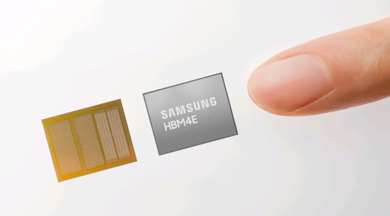
Samsung's currently disclosed 12-high HBM4E offers a capacity of 48GB, utilizing sixth-generation 10nm-class 1c DRAM process technology and Samsung Foundry's 4nm logic base die, with a stable operating speed of 14Gbps, expandable to 16Gbps, and a maximum per-stack bandwidth of approximately 3.6TB/s. The company is also planning a 32GB 8-high version and a 64GB 16-high version. If the 8-high product developed for NVIDIA's needs reaches 17–18Gbps, it will further enhance the operating speed of existing HBM4E.
NVIDIA officially launched NVHBM on August 26, positioning it as a custom HBM base die technology under the NVLink Fusion architecture, with co-design and validation conducted alongside memory manufacturers. According to data released by NVIDIA, NVHBM can deliver up to 30% higher per-stack memory bandwidth compared to standard HBM4E, reduce HBM power consumption by 15%, shrink the PHY and related support area by up to 67%, and free up to approximately 30% additional silicon area for the primary compute die. This technology is primarily aimed at custom XPU and CPU platforms leveraging NVLink Fusion.
The 8-high stacking also reduces complexity in the HBM back-end manufacturing process. As the number of HBM layers increases, DRAM dies require greater thinning and high-precision stacking, imposing stricter requirements on bonding, thermal dissipation, and yield control. In March this year, Samsung also showcased hybrid copper bonding technology for HBM products with 16 or more layers, targeting a reduction of over 20% in thermal resistance compared to traditional thermocompression bonding. The current 8-high solution, by contrast, reduces the number of stacked layers while boosting transfer speeds.
NVIDIA's HBM configuration for the next-generation Rubin Ultra is also being adjusted. TrendForce data indicates that NVIDIA used 12-high HBM4E as the baseline solution for Rubin Ultra from 2025 through the first half of 2026, and since the third quarter of this year has begun concurrently evaluating configurations such as 8-high HBM4E, 12-high HBM4, and 8-high HBM4, with final specifications yet to be determined. The adjustment is primarily driven by factors including DRAM supply tightness in 2027 and considerations around 12-high HBM4E validation and mass-production yields.
NVIDIA's disclosed Rubin Ultra system roadmap includes three NVLink scaling configurations—NVL72, NVL144, and NVL576—with NVL576 being the largest configuration; the next-generation Kyber rack design can accommodate 144 GPUs per rack and can be further expanded into larger NVLink compute domains.
Related Products
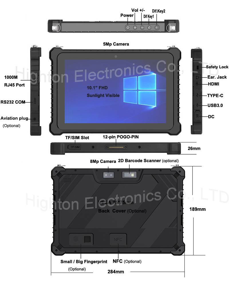

Hot Selling 10 Inch Intel N5100 I5 I7 FHD 8 +128GB 16+256GB Win10 Pro Win11 Pro 4G 5G Rugged Tablet PC Pad with NFC Barcode
Highton Electronics Co., Ltd.


Industrial and Commercial Point-Type Gas Detector
Jinan Benan Technology Development Co., Ltd.
TWP16 P-Band Tropospheric Wind Profile Radar
China Huayun Meteorological Technology Group Co., Ltd.



20 Inch 1600*900 Full HD 60Hz TFT LED Monitor with VGA and DP Interfaces for Desktop Computers-Business Use
Guangzhou Zanying Optoelectronics Technology Co., Ltd.