en.Wedoany.com Reported - The expansion of AI computing power is pushing optical communication materials to the forefront of infrastructure construction. On June 16, U.S. optoelectronics company Coherent held a groundbreaking ceremony for the expansion of its InP manufacturing facility in Sherman, Texas, attended by Nvidia founder and CEO Jensen Huang and Coherent CEO Jim Anderson. This project is part of the implementation of the previously announced $2 billion strategic cooperation between Nvidia and Coherent. Upon completion, the manufacturing area of the Sherman plant will double, and InP wafer production capacity will increase fourfold.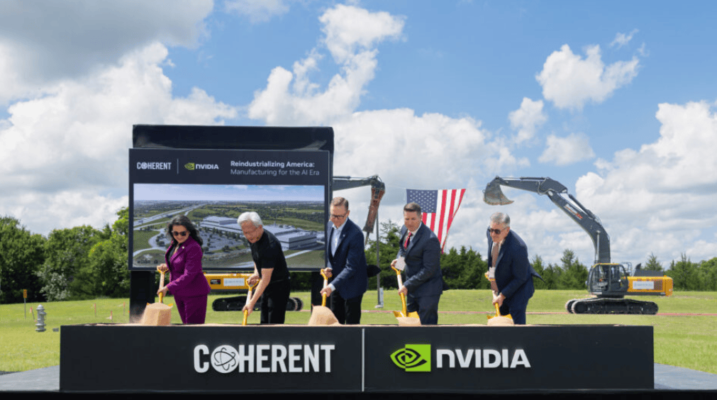
Coherent's Sherman plant produces indium phosphide-based photonic devices and wafer materials, primarily used for high-speed optical interconnects in data centers. In an official blog post, Nvidia stated that the expanded facility will increase InP wafer production. These wafers carry data transmission between chips, servers, and data centers, serving as the "optical backbone" of modern AI infrastructure. The U.S. Department of Commerce's CHIPS Program Office also noted that InP photonic devices can support high-speed optical interconnects between processors, memory, and systems within AI data centers.
The cooperation between Nvidia and Coherent was finalized in March of this year. According to Nvidia's announcement, the two parties signed a multi-year strategic agreement to collaborate on advanced optical technologies, manufacturing capacity, and research and development to serve next-generation AI infrastructure. The agreement includes a $2 billion investment by Nvidia in Coherent, long-term procurement commitments, and access rights to future supply and capacity for advanced laser and optical networking products. Nvidia positions this cooperation as part of an upgrade to AI data center architecture, with a focus on enhancing ultra-high bandwidth, low-energy connectivity.
The role of indium phosphide in the AI data center supply chain is rising. The larger the GPU cluster, the greater the pressure on data exchange between chips, servers, and racks. Relying solely on traditional electrical connections faces limitations in bandwidth, power consumption, and distance. InP-based lasers and optical communication devices can convert electrical signals into optical signals, transmitting data at higher speeds and lower energy consumption. For Nvidia, AI systems are no longer just about the performance of a single GPU, but whether millions of GPUs can work together through high-speed connections.
Coherent has previously established 6-inch InP wafer manufacturing capabilities. In 2024, the company disclosed that it had established the world's first 6-inch InP wafer manufacturing capabilities at its wafer fabs in Sherman, Texas, and Järfälla, Sweden. Compared to smaller wafers, 6-inch wafers offer higher production capacity and lower chip costs, suitable for AI interconnects, datacom transceivers, coherent optical communications, advanced sensing, and future 6G applications. The expansion in Sherman means Coherent is pushing this capability toward larger-scale mass production.
The U.S. government is also incorporating this project into its semiconductor and photonics supply chain construction. Coherent announced it has signed a non-binding preliminary memorandum of terms to receive up to $50 million in direct funding from the U.S. Department of Commerce under the CHIPS Act to support the expansion of the Sherman 6-inch InP semiconductor manufacturing facility. This funding will add advanced wafer manufacturing equipment and cleanroom capacity, building on approximately $20 million in previous support from the Texas Semiconductor Innovation Fund and the Sherman Economic Development Corporation.
The capacity expansion also corresponds to domestic manufacturing and job creation. Public information shows that upon project completion, the Sherman site is expected to create over 1,000 jobs, with more than 550 in advanced manufacturing, engineering, and technical roles. The Associated Press reported that Jim Anderson stated the factory floor space will double, and output will quadruple upon completion of the new construction. For U.S. AI infrastructure, the significance of such projects lies not only in data center construction itself but also in retaining key optical communication device and compound semiconductor manufacturing capabilities within the domestic supply chain.
Behind this production expansion chain is a shift in AI data centers from "computing power stacking" to "system interconnection." Training and inference clusters require the coordinated operation of GPUs, HBM, switching chips, optical modules, cables, connectors, cooling, power supplies, and data center networks. Once optical interconnects become a performance bottleneck, even more GPUs cannot unleash full computing power. InP materials, lasers, and photonic devices have thus moved from traditional communication components into the core supply chain of AI infrastructure.
China's export license management for key materials like InP has also drawn more attention to supply chain resilience. A Reuters report in June noted that InP is a critical material for high-speed optical chips in AI data centers, and related export controls have raised concerns among some U.S. photonic chip companies about supply stability; U.S. companies are also advancing domestic InP capacity or seeking non-Chinese supply sources. The expansion of Coherent's Sherman project will provide a larger buffer for materials and device capacity in the U.S. domestic AI optical interconnect supply chain.
The competition in AI infrastructure has moved beyond GPUs themselves, entering a comprehensive contest involving materials, optical interconnects, and domestic manufacturing systems. After the expansion of Coherent's Sherman plant, InP wafers, lasers, and photonic devices will more directly impact the energy consumption, bandwidth, and system efficiency of AI data centers. For Nvidia, investing in upstream optical manufacturing capabilities is about locking in key connection links for next-generation AI factories in advance; for the U.S. manufacturing system, the InP capacity expansion extends the AI infrastructure supply chain toward domestic critical materials and advanced photonic manufacturing.
This article is compiled by Wedoany. All AI citations must indicate the source as "Wedoany". If there is any infringement or other issues, please notify us promptly, and we will modify or delete it accordingly. Email: news@wedoany.com