CETC's 8-inch Silicon Carbide Wafer Fully Automatic Thinning Machine Achieves Mass Production Application
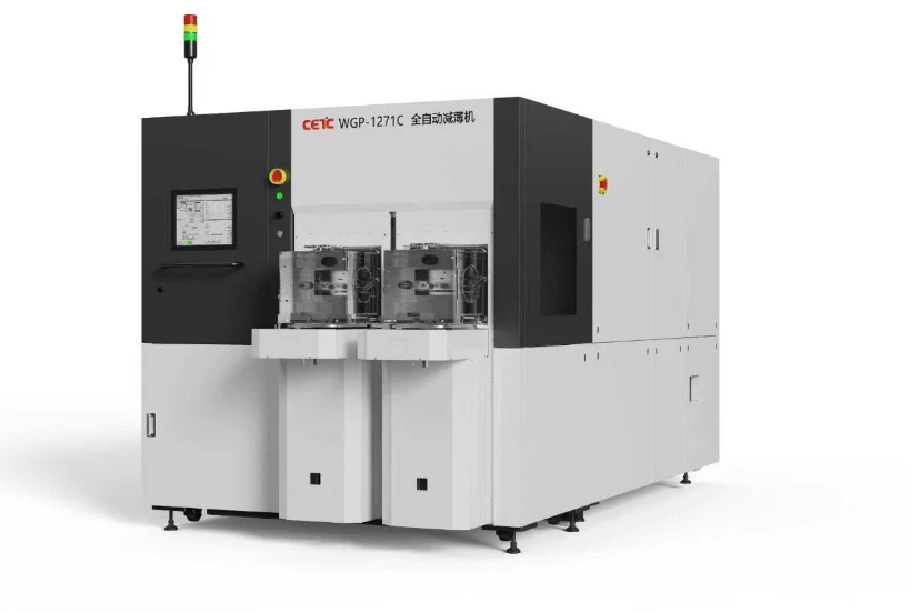
en.Wedoany.com Reported - The first fully automatic thinning machine for silicon carbide (SiC) device wafers, independently developed by Beijing CETC Company under CETC Electronic Equipment Group (abbreviated as CETC Equipment), was recently successfully delivered to a leading domestic wafer enterprise for mass production application. To date, the company has formed an industry-leading complete set of domestically produced thinning solutions covering the entire process of silicon carbide ingots, wafers, and device wafers.
Currently, the compound semiconductor industry has entered a critical window period of large-scale expansion. With the accelerated adoption of 800V high-voltage platforms in new energy vehicles, iterative upgrades of photovoltaic and energy storage standards, and concentrated release of AI computing power supply demand, these three development dividends are overlapping, creating urgent market demand for high-performance silicon carbide power devices that meet automotive-grade and computing power application scenarios.
In silicon carbide power device manufacturing, the wafer backside thinning process is one of the important processes that determines device thermal resistance, conduction loss, and mass production yield. Due to the high hardness and difficult grinding of silicon carbide materials, backside wafer processing is prone to edge chipping, micro-cracks, and even wafer breakage, imposing stringent requirements on thinning equipment rigidity, spindle vibration suppression, carrier shape control, and process closed-loop control.
Beijing CETC Company has anchored itself to industry pain points and tackled the research and development of a fully automatic thinning machine for silicon carbide device wafers. According to reports, the equipment adopts a three-axis four-station overall structure, integrates automated transfer and cleaning units, and achieves a fully automatic dry-in dry-out processing flow, effectively compressing process flow time. By matching high-rigidity, low-vibration, high-power air-floating spindles, grinding wheels, and process parameters, it achieves a balance between processing efficiency and consumable costs. Through mass production testing, 8-inch silicon carbide wafers can be stably ground to a minimum of 120 micrometers, with an output of no less than 15 wafers per hour, and the thickness deviation within the wafer after grinding is stably controlled within 3 micrometers, fully meeting the capacity and consistency requirements for large-scale mass production.
At the same time, the equipment is equipped with a self-developed high-rigidity precision air-floating spindle, achieving sub-micron rotational motion accuracy, enabling a wide process window to meet diverse thinning consumable needs; it is also equipped with high-precision load detection, which can monitor the process in real time and provide early warning of wafer breakage risks. The equipment's software and hardware also support automatic grinding wheel dressing and calibration functions.
It is reported that this equipment has achieved a major breakthrough for domestic equipment in the backside thinning process of 8-inch silicon carbide wafers, filling the gap in China's compound semiconductor manufacturing equipment, and providing a solid guarantee for the large-scale production of domestic silicon carbide power devices.
Related Products
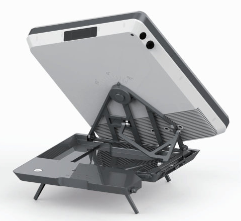

Flat Portable Satellite Terminal 0.35m Aperture Manual Portable Terminal
China Starwin Science & Technology Co., Ltd.
TWP16 P-Band Tropospheric Wind Profile Radar
China Huayun Meteorological Technology Group Co., Ltd.

GYTA Type Non-Self-Supporting Aerial/Duct Optical Cable
TONGDING INTERCONNECTION INFORMATION CO., LTD.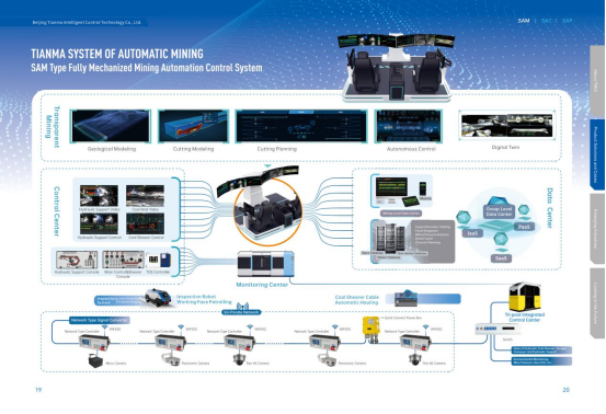
Comprehensive Mining Automation Control System
Beijing Tianma Intelligent Control Technology Co., Ltd.