BASF Signs Letter of Intent for Expansion of Semiconductor Materials Site in Taoyuan, Taiwan, China
en.Wedoany.com Reported - On October 20, the German chemical group BASF signed an investment letter of intent with the economic affairs authority of Taiwan, China, planning to expand its semiconductor materials production base in Guanyin District, Taoyuan City, adding semiconductor materials capacity for advanced processes below 2 nanometers. The project will be implemented by BASF's Electronic Materials business unit, with construction covering the expansion of advanced materials production facilities, enhancement of quality analysis capabilities, and expansion of the site's innovation center.
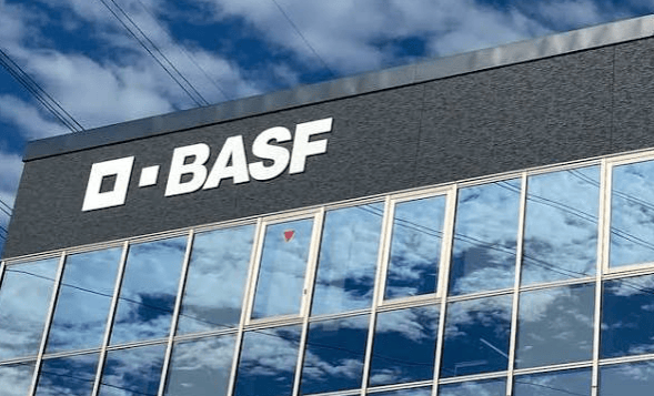
The investment letter of intent was signed by Liberman, Senior Vice President of BASF's Global Electronic Materials business and Chairman of BASF Taiwan, and Gong Mingxin, head of the economic affairs authority of Taiwan, China, during the 2026 Taiwan Global Investment Forum. The expansion focuses on the production and technology development of advanced high-purity specialty chemical formulations, as well as materials analysis and joint R&D capabilities for next-generation semiconductor processes. BASF plans to strengthen materials development collaboration with semiconductor manufacturing customers by expanding local manufacturing, quality assurance, and technical service facilities.
BASF's Electronic Materials business has operated in Taiwan, China, for more than 20 years, with existing products covering high-performance process chemicals for semiconductor and display manufacturing, customized chemical formulations, and specialized metal systems products for consumer electronics. In August 2025, BASF already announced arrangements for capacity expansion at the Guanyin site, upgrading of quality control facilities, and expansion of its R&D center, and established Taiwan, China, as the strategic operations base for its global Electronic Materials business. This signing further clarifies the related investment arrangements and the materials application direction for advanced processes below 2 nanometers.
Related Products
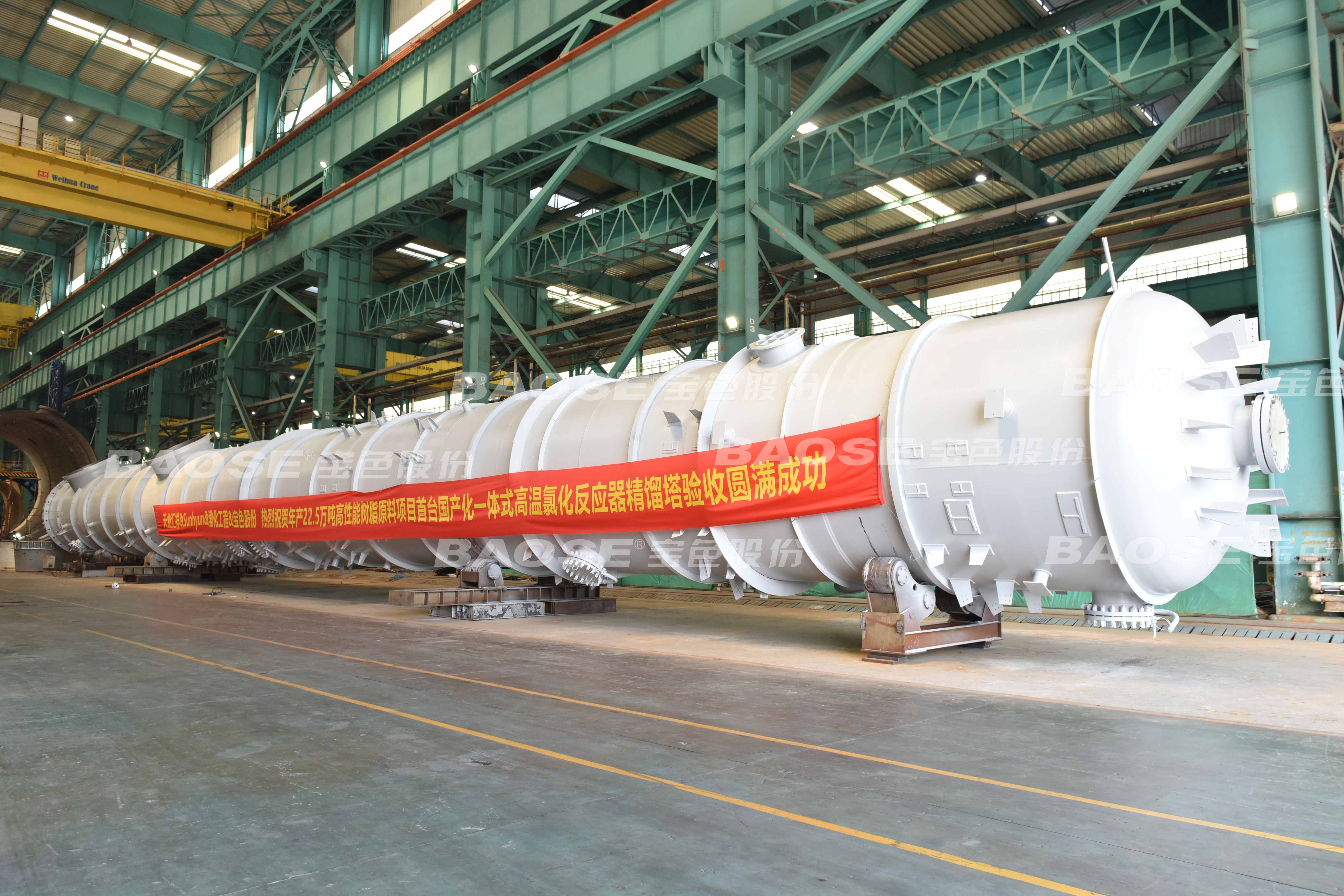

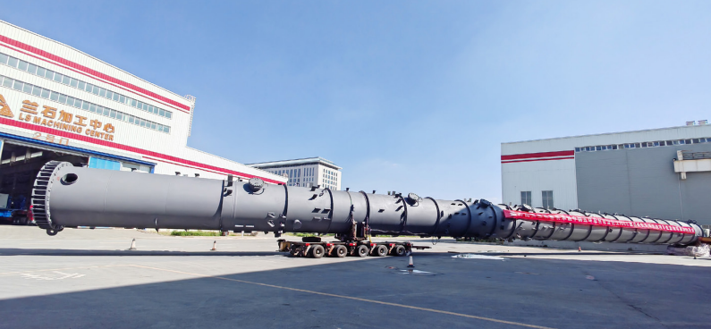
Integrated High-Temperature Chlorination Reactor Rectification Column
Nanjing Baose Co., Ltd.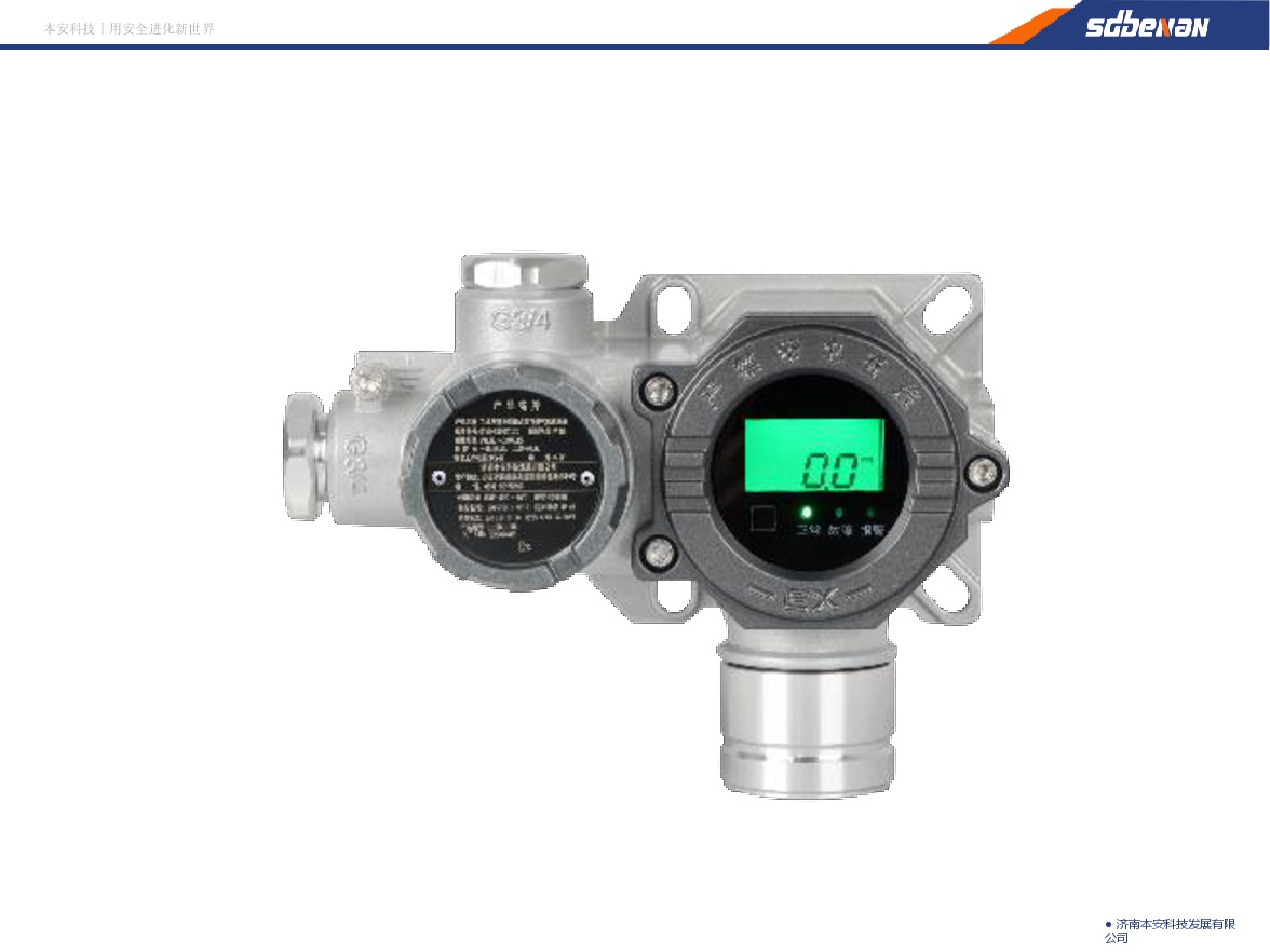
Industrial and Commercial Point-Type Gas Detector
Jinan Benan Technology Development Co., Ltd.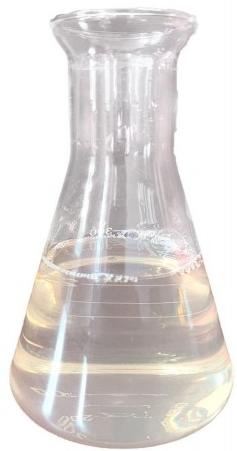
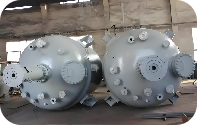
Hongxing Steel Chemical Pressure Vessel Steel Plate
Gansu JISCO Group Hongxing Iron and Steel Co., Ltd.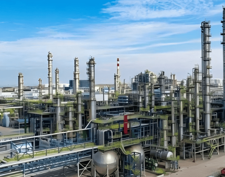
Steel Pipes for Refining and Coal Chemical Industries
YANGZHOU LONTRIN ENERGY EQUIPMENT CO.,LTD.
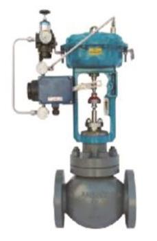
Quick-Change Single-Seat Control Valve / Quick-Change High-Pressure Single-Seat Control Valve
Beijing Consen Automation Technology Co., Ltd.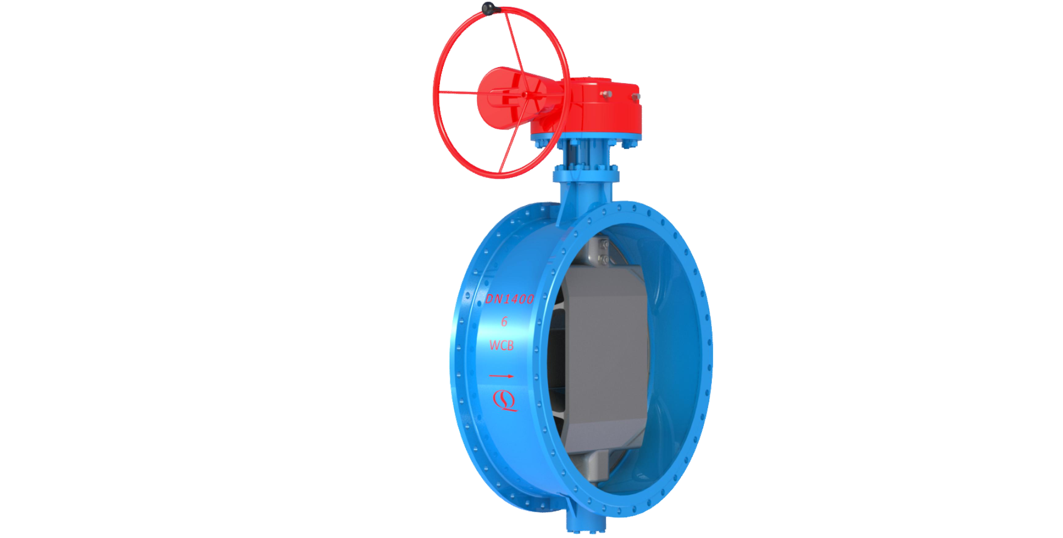
Bidirectional Metal Hard Sealed Seawater Butterfly Valve
Henan Quanshun Flow Control Science & Technology Co., Ltd.
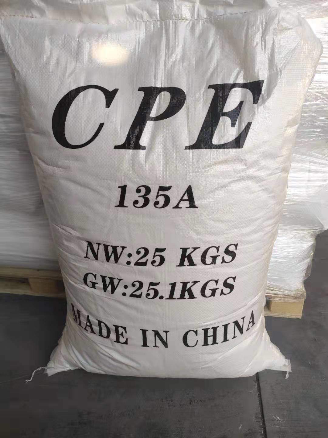
PVC Impact-Modified Chlorinated Polyethylene
Gansu Jinchuan Hengxin Polymer Technology Co., Ltd.