en.Wedoany.com Reported - Intel Foundry's research team showcased a pioneering GaN chiplet technology based on 300mm silicon wafers at the 2025 IEEE International Electron Devices Meeting. This technology integrates GaN power transistors with silicon-based digital control circuitry on the same chiplet, with a base silicon thickness of only 19 microns, approximately one-fifth the diameter of a human hair. This achievement has been included in the conference paper titled "GaN Chiplet Technology on 300mm Silicon Substrate."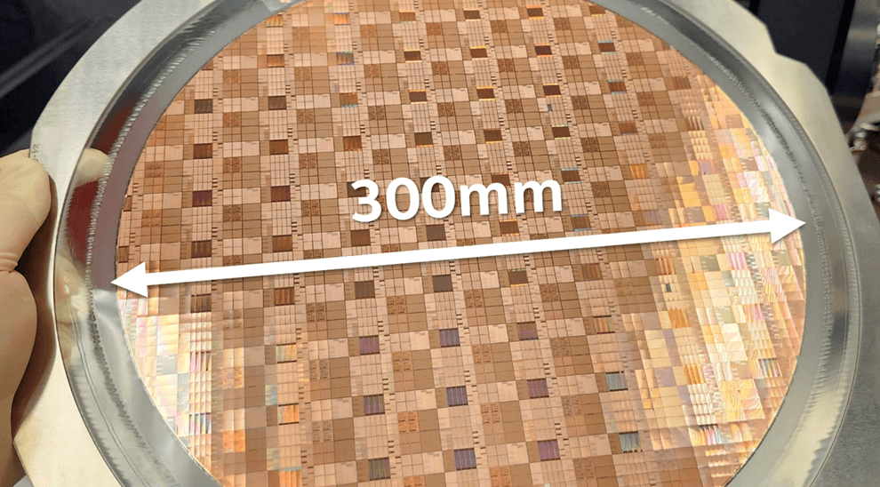
According to the Intel Foundry conference paper, this technology employs a pre-grinding stealth dicing process to achieve ultra-thin thinning on fully processed 300mm wafers, with the transistor electrical characteristics remaining unaffected after thinning. The GaN transistors with a gate length of 30 nanometers demonstrated a voltage blocking capability of 78 volts and an RF cut-off frequency exceeding 300 GHz. On the same chiplet, GaN N-MOSHEMT power transistors and silicon PMOS logic transistors were constructed side-by-side using a layer transfer process, connected with the same wiring layers to form complete digital circuit modules such as inverters, NAND gates, multiplexers, flip-flops, and ring oscillators. Ring oscillator measurement results showed a switching time of only 33 picoseconds per inverter, with performance uniformity maintained across the entire 300mm wafer.
This technology has been validated through four industry-standard reliability tests, including Time-Dependent Dielectric Breakdown, Positive Bias Temperature Instability, High-Temperature Reverse Bias, and Hot Carrier Injection. The test results indicate that the 300mm GaN MOSHEMT technology meets the reliability index requirements for practical products. Intel Foundry noted that GaN transistors switch faster and have lower energy loss, making them suitable for applications such as point-of-load power supplies in data centers, RF front-ends for wireless infrastructure, radar systems, and satellite communications. GaN's capability for efficient operation at frequencies above 200 GHz is well-suited for centimeter-wave and millimeter-wave frequency bands.
Compared to silicon-based technologies, GaN offers higher power density, enabling systems to achieve stronger functionality within a smaller form factor. GaN's wider bandgap supports stable operation at higher junction temperatures, reduces switching power loss, and decreases the size and cost of cooling systems. Intel Foundry utilizes standard 300mm silicon wafers for GaN production, which is compatible with existing silicon manufacturing infrastructure and is expected to reduce the additional investment required for large-scale mass production.
This article is compiled by Wedoany. All AI citations must indicate the source as "Wedoany". If there is any infringement or other issues, please notify us promptly, and we will modify or delete it accordingly. Email: news@wedoany.com