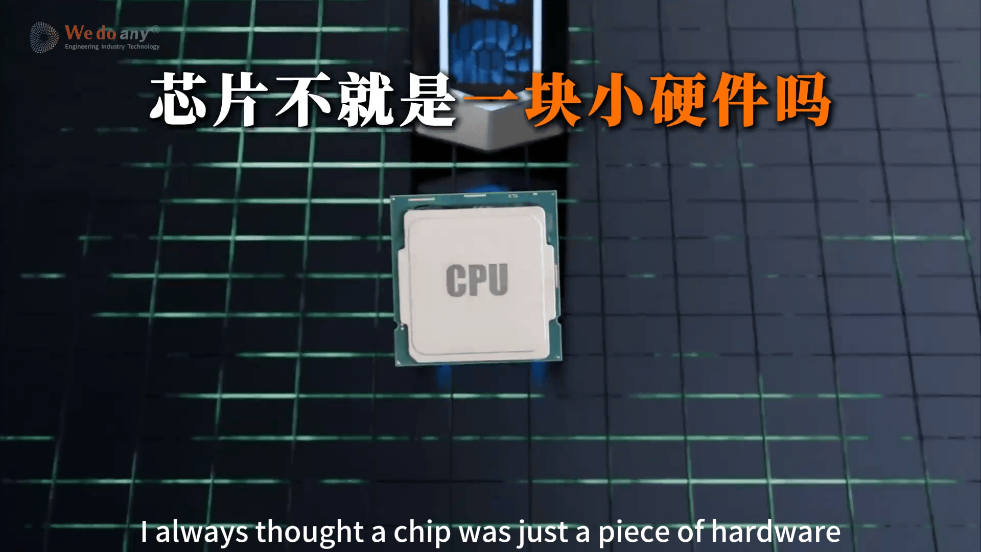
en.Wedoany.com Reported - Google Cloud officially launched the eighth-generation Tensor Processing Unit (TPU) at the Google Cloud Next 2026 conference in Las Vegas on April 22 local time. For the first time, it splits training and inference tasks onto two independent chips—TPU 8t is dedicated to AI model training, while TPU 8i is dedicated to AI inference services. In an official blog post, Amin Vahdat, Google's Senior Vice President and Chief Technology Expert for AI Infrastructure, stated that this architectural split stems from the significant divergence in training and inference workloads following the rise of AI agents: training pursues ultimate throughput and scale, while inference is more sensitive to latency and concurrency. 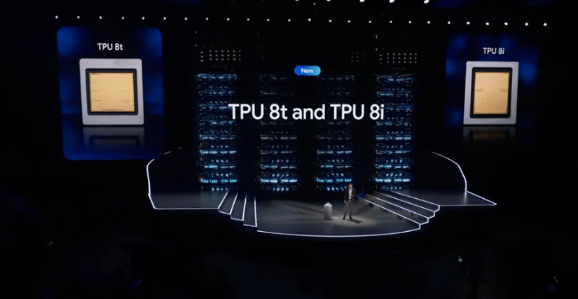
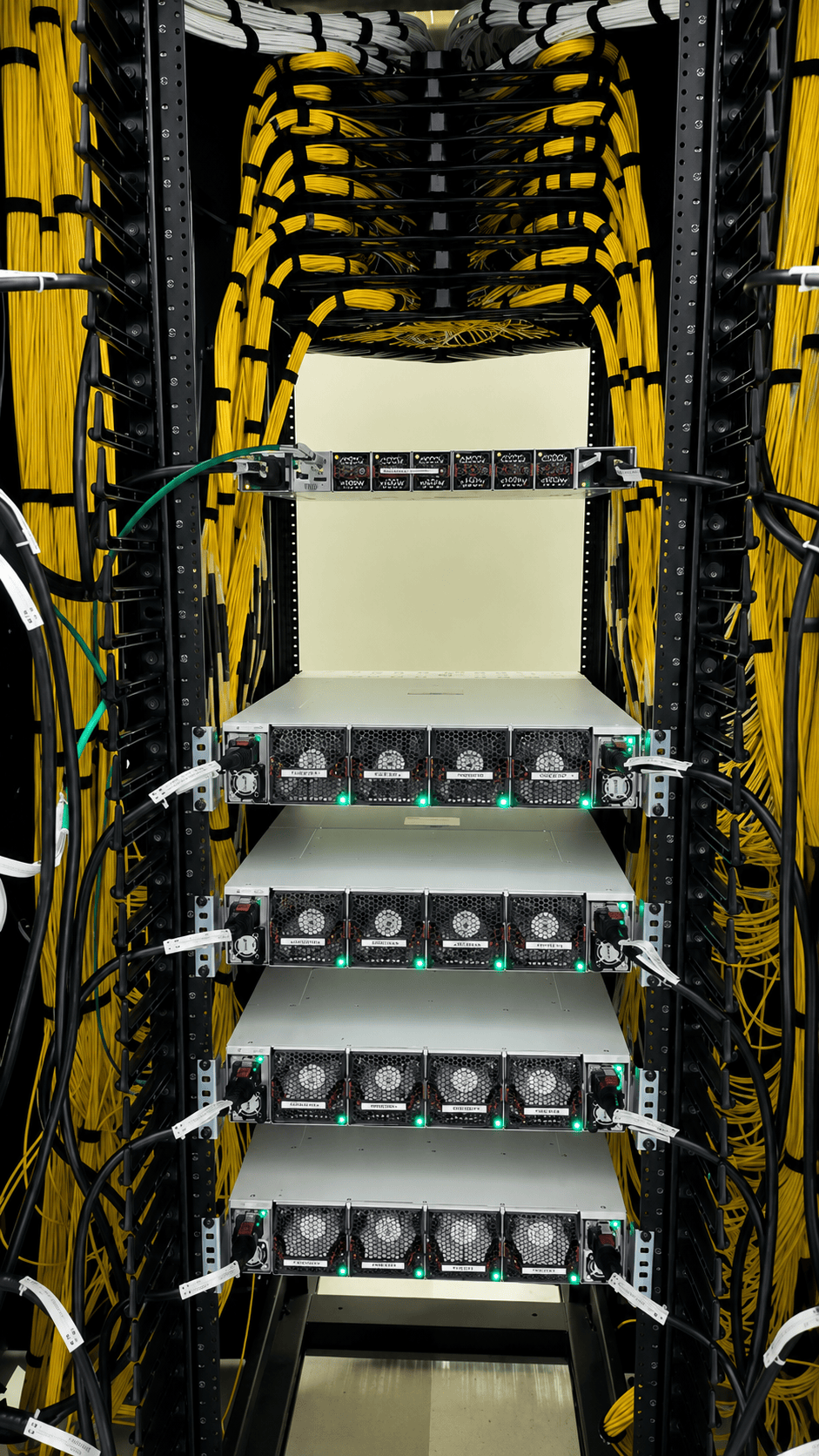
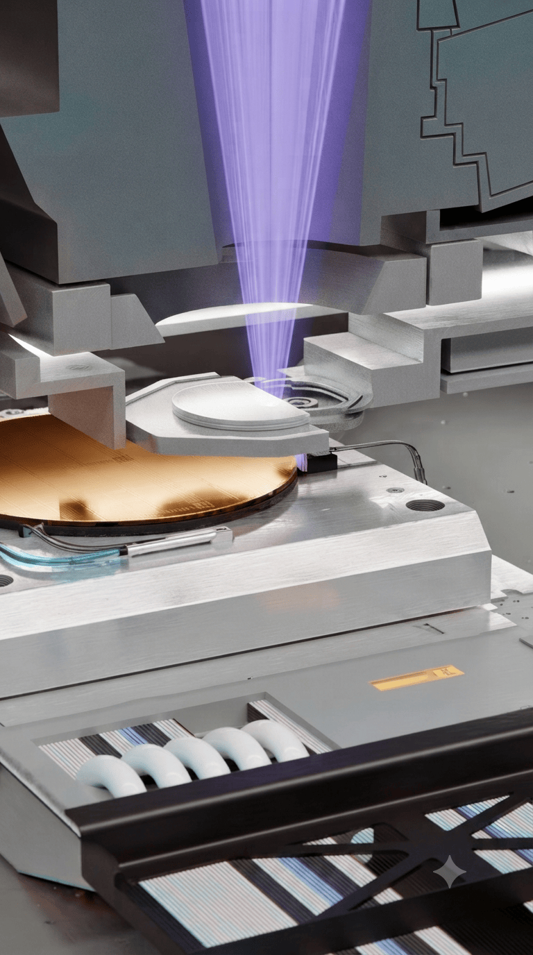
Positioned as a computing engine for large-scale training, the TPU 8t is equipped with 216GB of high-bandwidth memory (HBM), 6.5TB/s memory bandwidth, and 128MB of on-chip SRAM per chip, delivering a peak FP4 performance of 12.6 PetaFLOPS. The inter-chip interconnect bandwidth reaches up to 19.2 Tbps. A single TPU 8t cluster can scale to 9,600 chips, featuring 2PB of shared high-bandwidth memory and providing 121 ExaFlops of computing power. This represents a nearly 3x improvement in computational performance and up to a 2x improvement in performance per watt compared to the previous generation Ironwood. At the network level, the new Virgo architecture is introduced, quadrupling data center network bandwidth. A single network can connect over 134,000 chips, and combined with the Pathways framework, distributed training can scale to over 1 million chips in a single cluster. Google also simultaneously launched TPUDirect RDMA and TPUDirect Storage technologies, allowing data to bypass the CPU and be transmitted directly to TPU memory or high-speed storage, doubling the bandwidth for large-scale data transfers.
The TPU 8i targets high-concurrency inference scenarios, equipped with 288GB of high-bandwidth memory and 384MB of on-chip SRAM—the latter being 3x that of the previous generation Ironwood—enabling the model's active working set to reside entirely within the chip. This chip adopts the Boardfly hierarchical network topology, where communication between any two chips requires at most 7 hops, and introduces a collective acceleration engine that reduces collective communication latency by 5x. A single Pod can scale to 1,152 chips, delivering FP8 performance of 11.6 ExaFlops, with 331.8TB of HBM capacity per Pod. Compared to the previous generation, the TPU 8i offers an 80% improvement in price-performance and a 117% improvement in performance per watt. 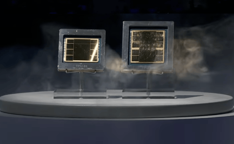
Both chips are powered by Google's self-developed Axion ARM architecture host processor, replacing the previous x86 architecture, and are supported by fourth-generation liquid cooling technology. In terms of software ecosystem, the TPU 8 series continues to support mainstream frameworks such as JAX, PyTorch, Keras, and vLLM, with native PyTorch support now in preview.
In a pre-recorded video, Google CEO Sundar Pichai reiterated that the company's capital expenditure in 2026 will reach $175 billion to $185 billion, a nearly sixfold increase from $31 billion in 2022, with over half of the machine learning computing power being directed to cloud services. Pichai also disclosed that 75% of new code generated internally at Google is now AI-generated and reviewed by engineers, a significant increase from 50% last autumn. This architectural split in TPUs represents a major strategic shift in Google's AI hardware approach, marking a new phase where AI chips move from "general-purpose for training and inference" to "task-specific, chip-specific."
This article is compiled by Wedoany. All AI citations must indicate the source as "Wedoany". If there is any infringement or other issues, please notify us promptly, and we will modify or delete it accordingly. Email: news@wedoany.com