en.Wedoany.com Reported - Advanced Micro Devices (AMD) officially announced on May 21 that its 6th generation AMD EPYC processor, codenamed "Venice," has begun production ramp-up. Utilizing TSMC's most advanced 2nm process technology, it becomes the industry's first 2nm high-performance computing product to enter the mass production stage. AMD also publicly revealed for the first time its successor product, "Verano," which will further expand its data center CPU product portfolio on the 2nm process.
AMD Chair and CEO Dr. Lisa Su stated in the official press release that Venice entering production ramp-up on TSMC's 2nm process is a key step in accelerating the deployment of next-generation AI infrastructure. She noted that as AI workloads rapidly expand from training and inference to increasingly complex Agentic scenarios, the CPU is becoming more critical in coordinating data movement, networking, storage, security, and system orchestration. TSMC Chairman and CEO Dr. C.C. Wei said in the same announcement that AMD's progress on TSMC's 2nm process demonstrates the importance of combining leading process technology with advanced design innovation.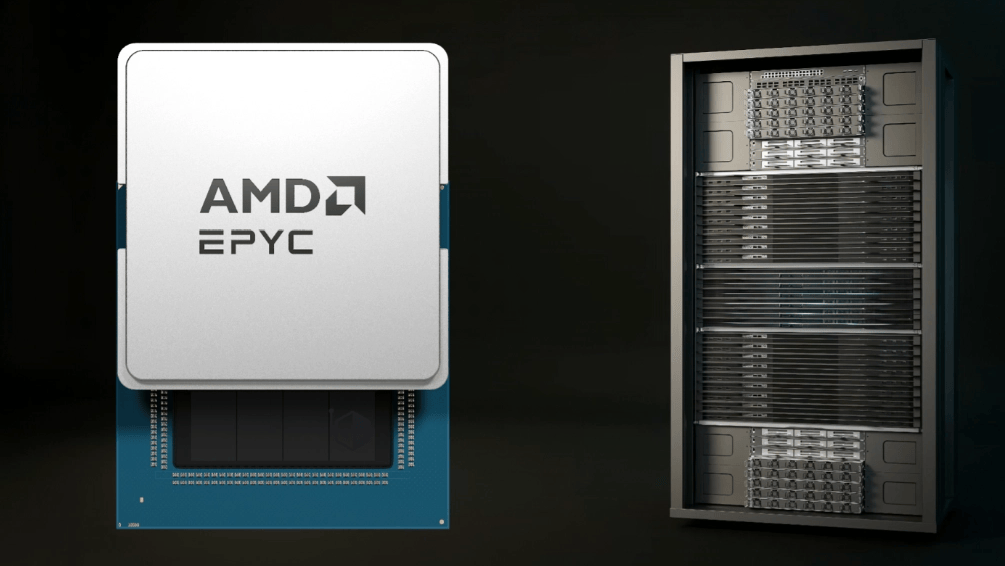
Venice is designed based on the new Zen 6 microarchitecture, configurable with up to 256 physical cores and supporting 512 threads, representing a 33% increase in core count over the previous generation EPYC Turin's 192 cores. According to technical indicators previously disclosed by AMD, Venice's overall performance can improve by up to 70% compared to the prior generation. This increase comes not only from the higher core count but also from improvements in per-core instruction execution efficiency, clock frequency, and other architectural enhancements. In terms of memory bandwidth, Venice boosts per-socket memory bandwidth to 1.6 TB/s, more than doubling the 614 GB/s of the current product line, thanks to support for up to 16 channels of DDR5 memory and compatibility with advanced memory technologies like MR-DIMM and MCR-DIMM.
On the I/O subsystem, Venice doubles the communication bandwidth between the CPU and GPU, expected to be achieved through the introduction of PCI Express 6.0. The new platform offers up to 128 PCIe lanes, with unidirectional data transfer rates reaching 128 GB/s, which has direct significance for the large-scale data exchange between processors and accelerators in AI training and inference. Venice will debut on AMD's new SP7 platform, a socket design that supports higher power delivery, providing the physical foundation for higher-density computing chip packaging.
AMD plans to offer Venice in two main versions: a standard Zen 6 version with up to 96 cores, and a high-density Zen 6c version scaling to 256 cores, both supporting 512 threads. The higher-density Zen 6c version has a Thermal Design Power (TDP) of approximately 600W, while the standard version is around 350 to 400W. Venice has started mass production at TSMC's factories in Taiwan, and AMD also disclosed future plans to introduce production of this product at TSMC's wafer fab in Arizona, USA.
The timing of Venice's production ramp-up coincides with a cycle where Agentic AI workloads are driving accelerated expansion in AI infrastructure deployment. As AI evolves from model training and online inference to Agentic scenarios requiring continuous autonomous decision-making, the role of the CPU in the data center is no longer limited to general-purpose computing but is taking on more load in task scheduling, data flow orchestration, security control, and system-level coordination. AMD explicitly positions Venice as the compute foundation for next-generation AI infrastructure.
In the Venice mass production announcement, AMD also publicly revealed its successor product, Verano, for the first time. Also based on TSMC's 2nm process, this product is an EPYC processor optimized around "performance per dollar per watt," specifically designed for cloud and AI computing workloads. AMD stated that Verano will introduce advanced memory innovations such as LPDDR memory to address the continuously growing demands for memory capacity and bandwidth from Agentic AI workloads. According to information previously disclosed by AMD executives in public forums, Verano is expected to launch in 2027, focusing on AI inference scenarios.
This article is compiled by Wedoany. All AI citations must indicate the source as "Wedoany". If there is any infringement or other issues, please notify us promptly, and we will modify or delete it accordingly. Email: news@wedoany.com