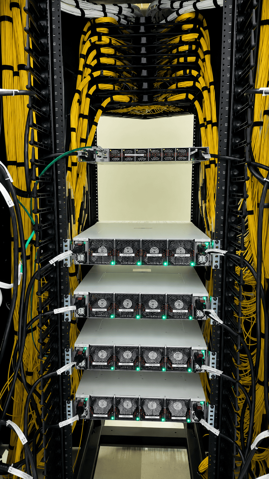
en.Wedoany.com Reported - On June 4, the Indian Institute of Technology Delhi and the US-based electronic design automation company Cadence announced the establishment of the IIT Delhi–Cadence Innovation Lab. This multidisciplinary innovation lab will provide platform support for cultivating semiconductor talent in India, AI-assisted chip design, EDA tool practice, and early-stage startup project incubation.
The lab's focus is on introducing industry-grade electronic design automation tools and AI-driven semiconductor design workflows into university research and talent development at an earlier stage. Cadence has long-standing expertise in chip design software, verification, packaging, system analysis, and intelligent system design, with its EDA tools widely used in integrated circuit design, verification, and pre-tapeout engineering processes. As one of India's premier engineering and technology institutions, IIT Delhi has a strong research foundation in electronics, electrical engineering, computer science, materials, artificial intelligence, and systems engineering. With the joint lab, students, researchers, and startup teams can engage in chip architecture exploration, design verification, prototype development, and AI-assisted design training within a toolchain closer to the industrial environment, helping bridge the gap between academic research and industrial design workflows.
The lab will also introduce an Early Master’s Research pathway for fourth-year undergraduate students at select IITs and NITs, co-supervised by Cadence experts and IIT Delhi faculty, and provide support for pre-seed stage startups to achieve first-time tapeout and working prototypes at low cost.
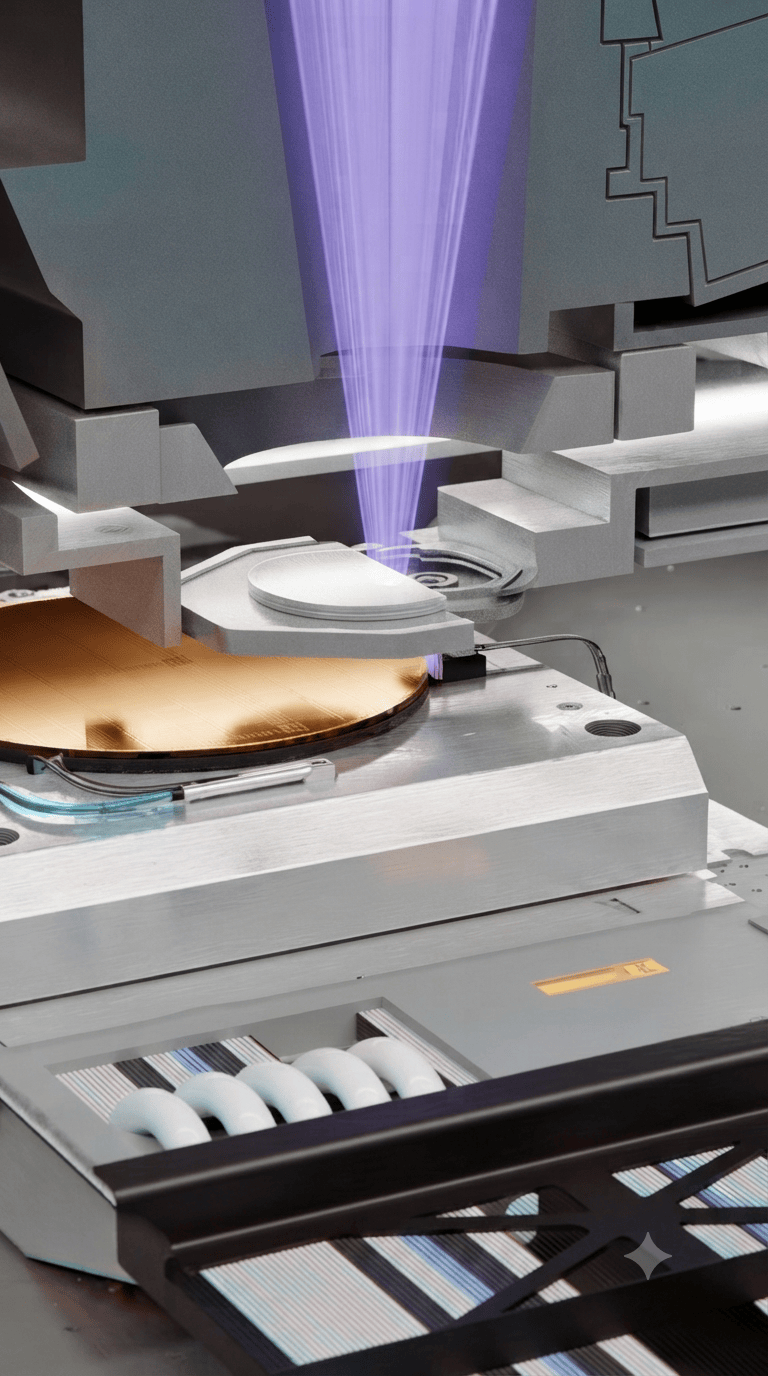
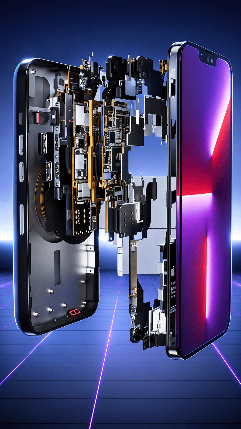
In recent years, India has been steadily advancing semiconductor manufacturing, chip design, and the development of its domestic electronics industry chain. Policies such as the India Semiconductor Mission and Design-Linked Incentive prioritize design capabilities, talent supply, and startup ecosystems. Competition in the chip industry is not limited to fabs and packaging facilities; front-end design, EDA tools, IP reuse, verification capabilities, and the density of engineering talent are equally critical in determining whether a country can consistently produce commercially viable chips. AI is transforming the semiconductor design process, from architecture exploration, placement and routing, verification and debugging, to power optimization, with an increasing number of stages requiring engineers to understand the interplay between algorithms, toolchains, and hardware constraints. The joint lab between IIT Delhi and Cadence helps embed these capabilities into education and early-stage R&D systems, cultivating talent in India ready to directly enter roles in chip design and intelligent system development.
This collaboration also provides a more practical engineering entry point for India's semiconductor startup teams. Many chip startups are constrained early on by tool costs, verification resources, mentor experience, and tapeout pathways. Even with application scenarios and algorithmic solutions, it is difficult for them to quickly transition from an idea to a silicon prototype. If the innovation lab can consistently provide EDA tools, design methodologies, industry mentors, and incubation support, it will help lower the barrier to trial and error for early-stage projects, fostering more indigenous design initiatives in areas such as wearable devices, the Internet of Things, communication chips, AI accelerators, and edge computing. The subsequent impact will depend on the lab's scope of access, the quality of courses and research projects, the number of startup teams onboarded, and whether it can truly form a closed loop from talent development to prototype verification and industrial collaboration.
This article is compiled by Wedoany. All AI citations must indicate the source as "Wedoany". If there is any infringement or other issues, please notify us promptly, and we will modify or delete it accordingly. Email: news@wedoany.com