en.Wedoany.com Reported - A collaborative effort between China's Zhejiang University and Australia's RMIT University has resulted in the development of a driven imaging chip based on nanofabrication technology. This chip enables cameras and sensing systems to detect details far beyond the range of traditional color imaging, including subtle differences in materials and environments that are indistinguishable to the human eye. The research findings have been published in Nature Electronics.
The study demonstrates a method of integrating light analysis directly into imaging hardware, rather than relying on separate laboratory instruments. The researchers state that the nanofabrication-based design allows for the direct capture of spectral information at the imaging point, thereby supporting applications such as machine vision, automated inspection, and environmental monitoring.
The research team notes that while cameras are highly efficient at capturing images, applications like machine vision, automated inspection, and environmental monitoring depend not only on an object's appearance but also on understanding different colors and wavelengths. This information can reveal differences in materials or surface conditions that appear identical under standard imaging.
Distinguished Professor Baohua Jia from RMIT's Centre for Atomaterials and Nanomanufacturing, collaborating with a team led by Professor Jianrong Qiu from Zhejiang University, contributed expertise in nanofabrication, optical characterization, and device testing. Dr. Han Lin from RMIT also participated as a co-author.
Professor Jia stated that this approach goes beyond traditional post-processing techniques. "This isn't about adding more image processing after the fact; it introduces a new physical component that can separate light at a very small scale, close to the sensor itself."
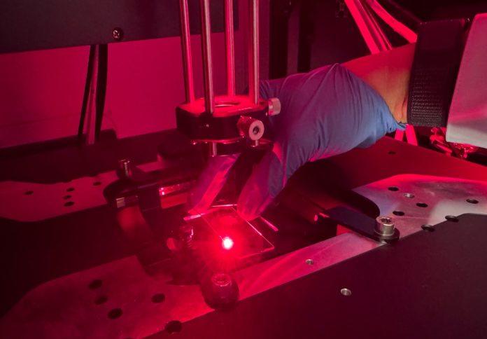
The device utilizes ultrafast laser pulses to create spiral microstructures inside transparent materials. These microstructures act as miniature spectrometers, breaking down incoming light into patterns readable by the sensor, thus enabling compact spectral analysis without external equipment.
The researchers demonstrated a prototype by integrating this structure with a commercial image sensor, proving its ability to capture spectral information and support microspectral imaging from visible to near-infrared wavelengths.
Dr. Lin stated that these achievements mark a significant step in translating the concept into a usable technology, helping to "shift the discussion from theoretical possibilities to the types of sensing systems that could actually be built in the future."
Professor Qiu noted that the work is still in its early stages but demonstrates a viable path for compact sensing systems. "Proving that a concept works at the chip level is a crucial step."
The researchers indicate that future work will focus on scaling up the fabrication method, testing more materials, and optimizing reconstruction software to improve the way light information is interpreted from the chip.
This article is compiled by Wedoany. All AI citations must indicate the source as "Wedoany". If there is any infringement or other issues, please notify us promptly, and we will modify or delete it accordingly. Email: news@wedoany.com