Sony and TSMC Plan to Invest 1 Trillion Yen in Mass-Producing Image Sensors
en.Wedoany.com Reported - On August 10, Sony Semiconductor Solutions Corporation, under Sony Group, and TSMC plan to invest approximately 1 trillion yen (about $6.32 billion) in a next-generation image sensor project, with plans to establish a joint venture in which Sony holds approximately 60% and TSMC holds approximately 40%, with commercial production slated to begin as early as 2029.
The two parties signed a non-binding memorandum of cooperation in May, planning to establish a Sony-controlled joint venture in Japan and equip a new wafer fab in Kōshi City, Kumamoto Prefecture, with R&D and production lines. The establishment of the joint venture remains subject to the signing of a legally binding definitive agreement and the satisfaction of customary closing conditions.
The project will combine Sony's sensor design capabilities with TSMC's semiconductor process and manufacturing capabilities to develop and produce next-generation image sensors. In addition to applications such as smartphones and automobiles, the two parties will also assess sensor demand in physical AI fields, including automotive and robotics.
In April, Japan's Ministry of Economy, Trade and Industry approved subsidies of up to 60 billion yen for Sony's image sensor fab in Kōshi City. The fab's planned capacity is equivalent to 10,000 300mm wafers per month, with shipments scheduled to begin in May 2029. Related investments are planned to be implemented in phases based on market demand and are subject to Japanese government support.
Sony declined to comment on the 1 trillion yen investment amount, specific shareholding ratio, and mass-production schedule disclosed by Nikkei, while TSMC had not responded as of the time of Reuters reporting. The two parties will continue to discuss the investment plan and definitive agreement, with the specific scale and implementation timeline subject to the formal agreement.
Related Products

Industrial and Commercial Point-Type Gas Detector
Jinan Benan Technology Development Co., Ltd.

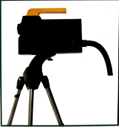
Automatic Aiming Laser Remote Obstacle Removal Robot
Pinggao Group Weihai High-Voltage Apparatus Co., Ltd.
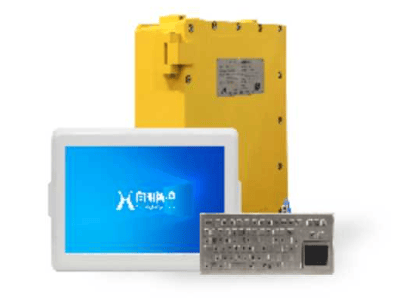
KJD127(A) Mining Explosion-Proof and Intrinsically Safe Computer
Taiyuan Xiangming Intelligent Control Technology Co., Ltd.

Multi-function Marine Monitoring Low-altitude Detection Radar Sea-air Boundary Ocean Dynamic Environment Measurement
Chengdu Dixin Technology Co., Ltd.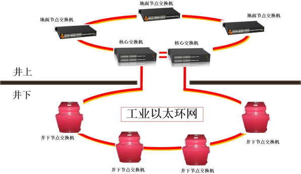
Mine Explosion-proof and Intrinsically Safe Industrial Ethernet Ring Network (10 Gigabit/Gigabit)
Chongqing Mas Sci&Tech Co., Ltd.