en.Wedoany.com Reported - On the morning of August 11, Vertilite's high-end optical communication chip and device R&D and manufacturing base was signed in Changzhou, Jiangsu. The project signed this time plans a cumulative investment of approximately 5 billion yuan, focusing on the construction of R&D and mass production lines for high-end indium phosphide laser chips. The project is currently at the signing stage.
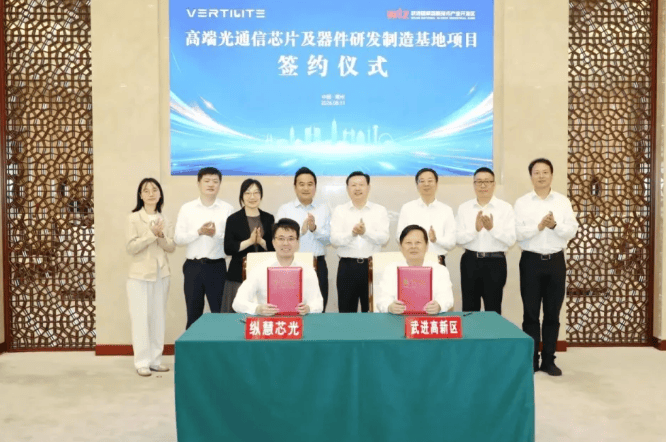
The new base will focus on the R&D and large-scale mass production of high-end indium phosphide laser chips, with construction content covering the optical chip R&D and manufacturing processes. Based on this project signing, Vertilite will continue to increase R&D and production investment to promote the industrialization of related products.
Founded in 2015, Vertilite adopts an IDM model integrating chip design, epitaxial growth, wafer manufacturing, and packaging and testing, and has established manufacturing capabilities for gallium arsenide and indium phosphide optical chips. The company's products are mainly used in consumer electronics 3D sensing, automotive-grade LiDAR, and high-speed optical communications.
The company entered Changzhou Wujin National High-Tech District in 2018. In September 2025, Vertilite's high-end optical communication chip project, built with an investment of 550 million yuan, was completed and put into operation locally. The project covers an area of 40 mu, with a building area of approximately 28,000 square meters, establishing large-scale production capacity for gallium arsenide and indium phosphide chips.
The approximately 5 billion yuan project signed this time represents new investment implemented by Vertilite in Changzhou. The project's investment scale, construction content, and signing time all differ from the 550 million yuan project that went into operation in 2025. The new production lines will further target the R&D and mass production of high-end indium phosphide laser chips.