en.Wedoany.com Reported - VIEW Micro Metrology is advancing a series of internal and customer-driven measurement studies at system laboratories in the United States and Asia, with the relevant application engineering teams currently in the research phase.
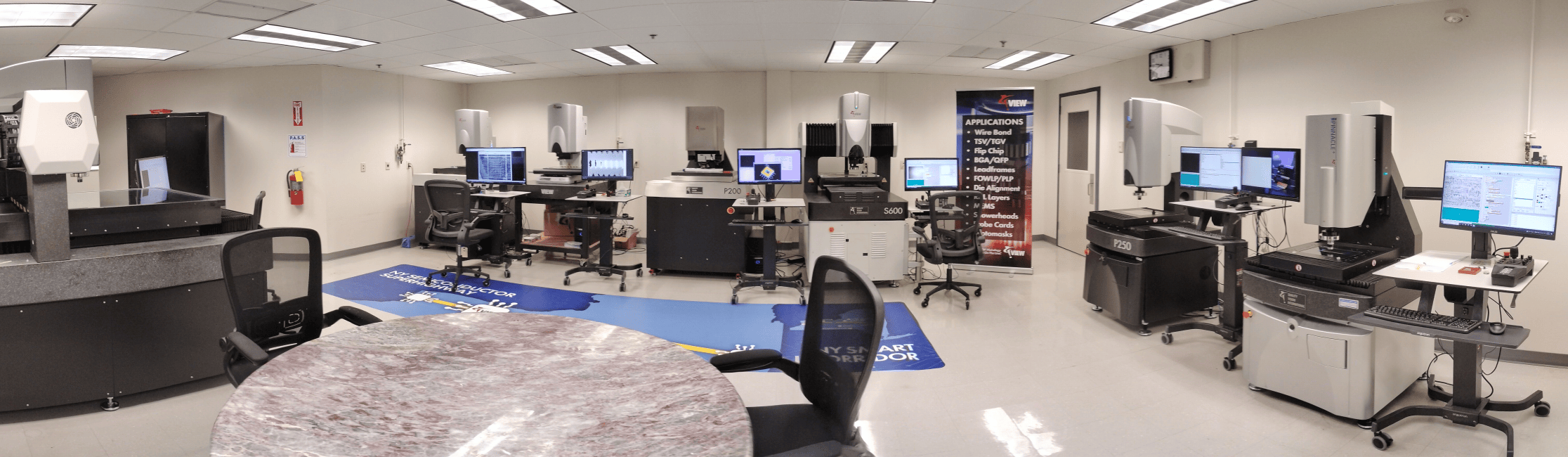
The VIEW Micro Metrology System Evaluation Laboratory in Rochester, New York, is equipped with a full range of VIEW dimensional metrology tools. This facility supports both internal development efforts and real-world customer applications, providing technology validation and process optimization for advanced semiconductor packaging and other manufacturing environments.
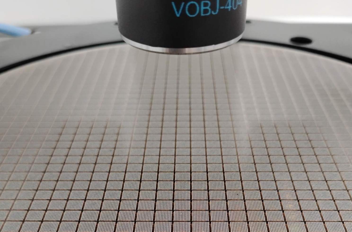
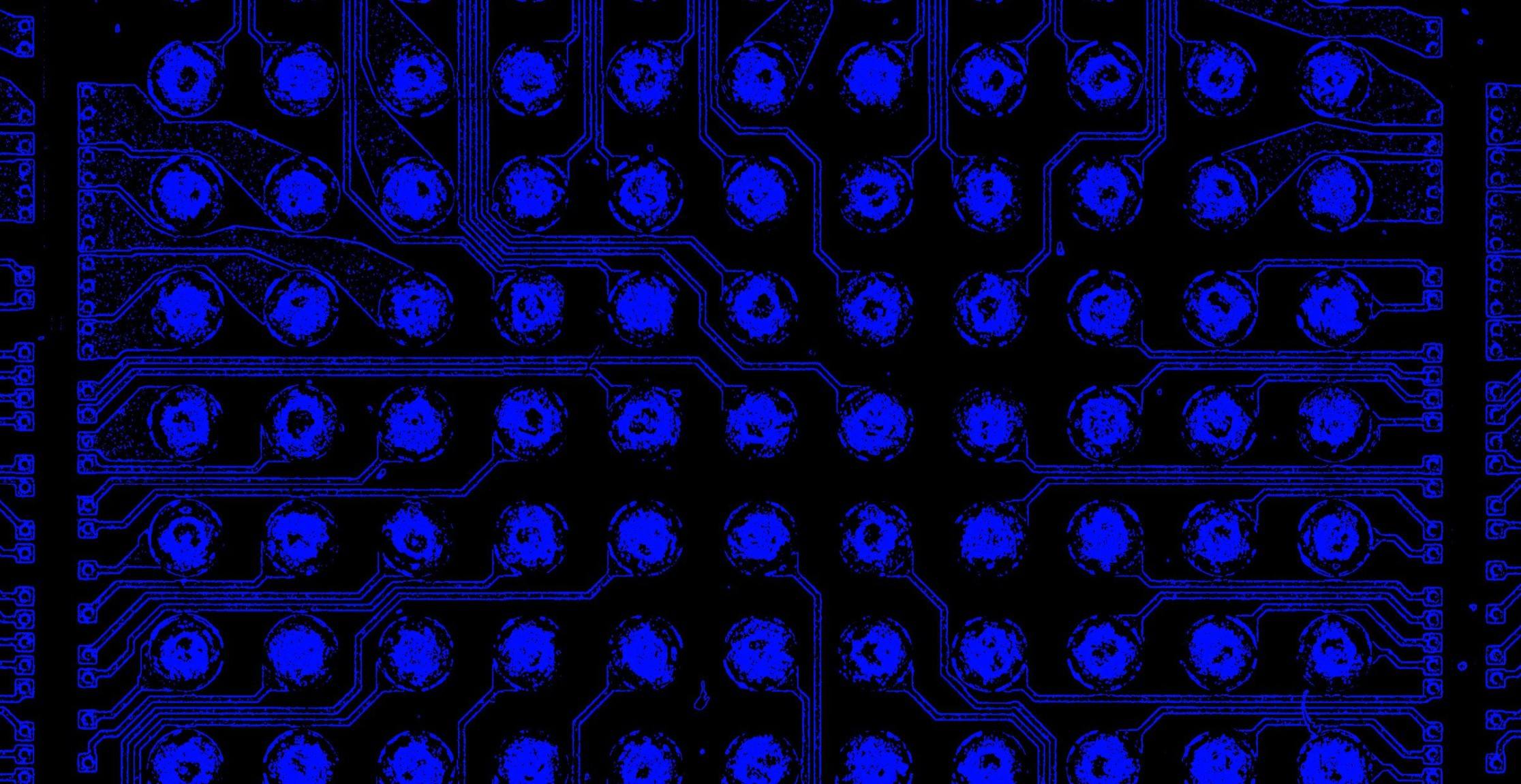
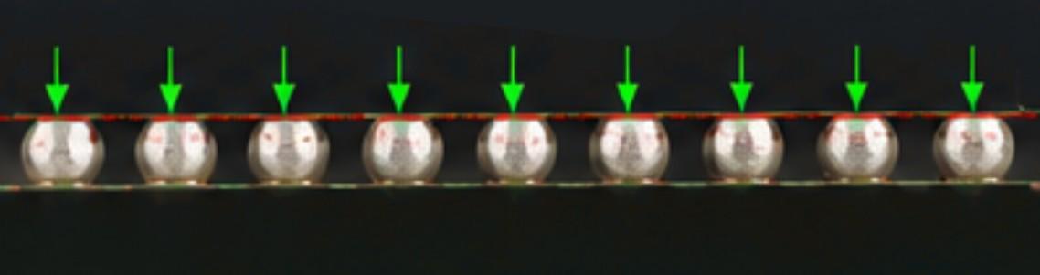
A key study focuses on the measurement throughput of ball grid array (BGA) chips on 200 mm wafers. Each wafer contains approximately 1300 chips, with each chip comprising 110 solder balls. The objective of this study is to evaluate measurement efficiency and data quality in high-volume inspection scenarios, with key areas including: comparing cycle time differences between "Move and Measure" (MAM) and "Continuous Image Capture" (CiC™) stroboscopic recipes for individual solder ball dimensions; detecting ball position defects on the wafer; comparative analysis of ball Z-height measurements using through-the-lens (TTL) laser and area multi-focus (AMF™) 3D imaging; and repeatability assessment across 25 wafers within the same batch. Results are expected to be published by late summer this year.
In addition to wafer-level studies, the laboratory is also involved in a gas distribution plate project, a component used in wafer deposition processes, analogous to a semiconductor "showerhead." A similar component for the aerospace sector is also under investigation. The through-holes on the gas distribution plate typically have diameters greater than 250 µm, which falls within the capability of VIEW measurement systems. However, inspection challenges arise from requirements for feature uniformity, true position and pitch accuracy, surface topology, and overall positional precision. Defect detection is also necessary, including identifying clogged or partially clogged holes, micro-cracks, pits, residue accumulation, and surface contamination. Throughput is a critical consideration for such applications, involving whether the inspection tool can achieve the measurement speed required for in-line production and whether manufacturers can achieve 100% inspection without sacrificing quality.
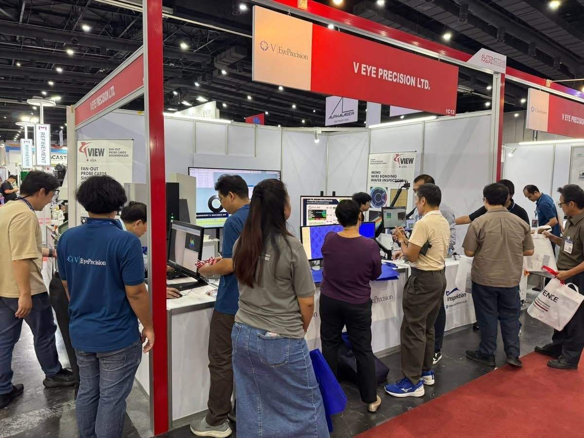
In Asia, VIEW's authorized representative, V Eye Precision, continues to expand application development in the BGA and optical transceiver markets in Thailand, supporting customers in Thailand, Singapore, the Philippines, and Indonesia. BGA-related work primarily focuses on ball height and coplanarity measurements, key parameters for ensuring reliable electrical connections and downstream assembly yields. Concurrently, V Eye is advancing metrology applications for optical transceiver manufacturing. Optical transceiver devices integrate sub-micron photonic structures, fiber optic interfaces, and precision packaging, demanding extremely tight alignment tolerances, where even a ±1 µm offset can significantly impact optical coupling efficiency.
VIEW's aforementioned research aims to help customers drive higher throughput, improve yields, and achieve reliable, scalable inspection in advanced packaging environments. By enabling precise, traceable 3D measurements, VIEW metrology transforms inspection from a passive quality gate into an active engineering tool, allowing customers to detect subtle process drifts and reduce rework.

VIEW Micro Metrology is a company providing high-performance, high-precision integrated metrology solutions designed for use on or near the production line, primarily serving the semiconductor, electronics, and medical sectors. Its solutions leverage advanced non-contact optical metrology systems and versatile software to achieve precise, high-throughput applications. All solutions are turnkey and supported by collaborative design and production integration support.
This article is compiled by Wedoany. All AI citations must indicate the source as "Wedoany". If there is any infringement or other issues, please notify us promptly, and we will modify or delete it accordingly. Email: news@wedoany.com