China's Yuquan Launches 10,000-Channel 3D Nano Laser Direct Writing Lithography Machine
en.Wedoany.com Reported - Hangzhou Yuquan Precision Instruments Co., Ltd. (Yuquan), in collaboration with the State Key Laboratory of Extreme Photonics and Instrumentation at Zhejiang University, recently launched the "10,000-Channel 3D Nano Laser Direct Writing Lithography Machine." This equipment provides foundational technological support for high-end masks, photonic chips, metasurfaces, and other semiconductor and micro-nano manufacturing fields.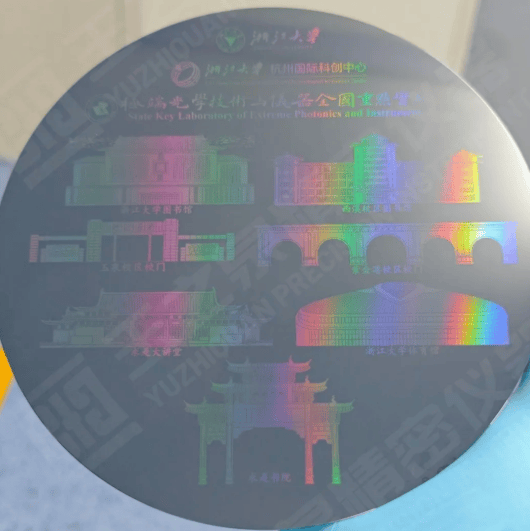
Founded in December 2022 and headquartered in Hangzhou, China, Yuquan's founding shareholders consist of scientific researchers with years of deep expertise in optics and entrepreneurs with extensive corporate management experience, dedicated to solving the nation's "bottleneck" lithography technology challenges.
Although two-photon laser direct writing technology offers high processing precision, it is limited by the physical constraints of single-beam scanning, making it difficult to meet the demands of large-area, high-efficiency industrial production. Yuquan's R&D team proposed a "10,000-channel rapid independent modulation scheme," capable of instantly generating over 10,000 independently controllable parallel laser focal points. Combined with intelligent global optimization algorithms, the intensity uniformity of the focal point array is improved to over 95%, breaking through the efficiency bottleneck of traditional single-beam scanning.
The equipment excels in performance: it achieves an ultra-high printing rate of over 200 million voxels per second; under specific processes, the minimum feature size can reach sub-50nm; the 2D surface scanning rate reaches 40 mm²/min, dozens of times faster than traditional technologies, and the maximum processing area can fully cover a 12-inch wafer.
In addition to applications in high-end mask micro-nano manufacturing fields such as photonic masks, DOE masks, and MEMS masks, the equipment is also suitable for customized, small-batch processes requiring rapid iteration. Application scenarios include photonic chips and advanced packaging, supporting customized, small-batch R&D of high-precision chips; MEMS sensors and microfluidic devices, enabling rapid prototyping of complex 3D microstructures; and precision optical components, meeting stringent requirements in optical anti-counterfeiting and optical communication fields such as metalenses and DOE devices.
The equipment also provides core manufacturing tools for large-scale production of cutting-edge fields like metasurfaces. As core components for future AR/VR, LiDAR, and 6G communications, traditional processing of metasurfaces often takes weeks, while the 10,000-channel technology can drastically compress the processing cycle to just a few hours. Currently, metasurfaces have become the first processing category where this equipment has been deployed and demonstrates clear advantages, driving the commercialization of related frontier industries.
Related Products

Automatic Aiming Laser Remote Obstacle Removal Robot
Pinggao Group Weihai High-Voltage Apparatus Co., Ltd.
Flat Portable Satellite Terminal 0.35m Aperture Manual Portable Terminal
China Starwin Science & Technology Co., Ltd.


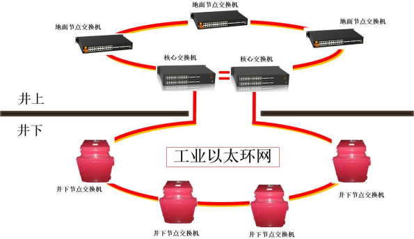
Mine Explosion-proof and Intrinsically Safe Industrial Ethernet Ring Network (10 Gigabit/Gigabit)
Chongqing Mas Sci&Tech Co., Ltd.