Samsung of South Korea Plans to Use TSMC's 3nm Process to Produce NVIDIA Custom HBM Chips
en.Wedoany.com Reported - On October 18, South Korean semiconductor industry sources indicated that Samsung Electronics plans to use TSMC's 3nm process to produce the base dies for NVIDIA's next-generation custom high-bandwidth memory, NVHBM. NVIDIA has required Samsung Electronics, SK Hynix, and Micron to uniformly adopt TSMC's 3nm process for manufacturing base dies and to use the sixth-generation 10nm-class 1c DRAM process for producing core memory dies. Samsung is said to have accepted the requirements after internal review, and the two parties plan to collaborate for the first time in the HBM chip manufacturing process.
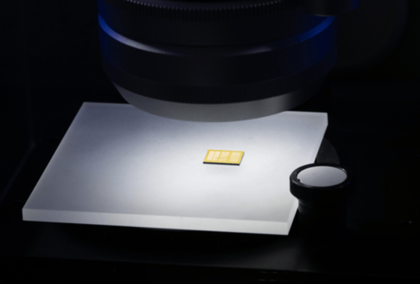
Samsung previously adopted a self-manufacturing model, with its foundry business producing HBM base dies and its memory business responsible for core die manufacturing. Currently, Samsung's HBM4 and HBM4E products, the latter of which is undergoing mass production validation, both use its own 4nm process to manufacture base dies, while core dies are produced on the 1c DRAM lines at its Hwaseong and Pyeongtaek plants. According to the plan disclosed this time, Samsung will continue to retain the self-manufacturing model for standard HBM and custom products for other customers such as AMD.
NVIDIA launched NVHBM technology on August 26, integrating a custom memory controller into the HBM base die. According to the architecture design it published, compared with standard HBM4E, NVHBM can increase single-stack memory bandwidth by up to 30%, reduce HBM power consumption by 15%, and free up up to 25% of the XPU compute chip area. NVIDIA plans to have multiple memory suppliers provide NVHBM products using a unified architecture, reducing adaptation and validation work across products from different vendors.
Samsung and TSMC had previously cooperated on compatibility around the advanced packaging process required to connect HBM to graphics processors. The proposed manufacturing arrangement this time extends the cooperation to base die production. South Korean semiconductor industry personnel also revealed that Samsung is validating the feasibility of using its own 2nm foundry process to manufacture NVHBM base dies, in order to address possible supply capacity constraints on TSMC's related production lines in the future.
Related Products



20 Inch 1600*900 Full HD 60Hz TFT LED Monitor with VGA and DP Interfaces for Desktop Computers-Business Use
Guangzhou Zanying Optoelectronics Technology Co., Ltd.
Automatic Aiming Laser Remote Obstacle Removal Robot
Pinggao Group Weihai High-Voltage Apparatus Co., Ltd.

MUX Series Communication Interface Device for Security and Stability Control System
Nanjing NR Electric Co., Ltd.
JiuTian OneSky Pilot—Intelligent Management And Service Platform
China Times Prospect Science & Technology Co., Ltd.