

Recently, a research team from ETH Zurich, in collaboration with Empa and led by Maksym Kovalenko, proposed a novel image sensor solution based on perovskites, an innovation that has the potential to revolutionize color recognition and imaging technology.
In traditional silicon image sensors, each pixel can only capture about one-third of the available light because color filters are required to distinguish colors. However, researchers from Kovalenko's team discovered that the physical properties of lead halide perovskite crystals change with their chemical composition, allowing them to identify different colors of light without the need for filters. By adjusting the content of iodine, bromine, and chlorine in the perovskite, they were able to create pixel layers that absorb red, green, and blue light, respectively. These pixel layers can be stacked in the image sensor, thereby improving light capture efficiency and spatial resolution.
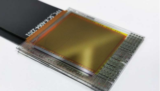
"We are further developing this technology, moving from a rough proof-of-concept stage to practical applications," Kovalenko stated. His team has successfully built two fully functional thin-film perovskite image sensors and demonstrated that these sensors outperform traditional silicon technology in light sensitivity, color reproduction accuracy, and resolution. Additionally, perovskite image sensors can eliminate certain artifacts in digital photography, such as demosaicing and moiré patterns.
Beyond consumer digital cameras, perovskite image sensors show great potential in the field of machine vision. Particularly in hyperspectral imaging, researchers can precisely control the wavelength range absorbed by each layer, thereby defining more clearly separated color channels. This is of significant importance for applications such as medical analysis, agriculture, and automated environmental monitoring.
Although perovskite image sensors are still in the early stages of research and development, the researchers have already proven the feasibility of their miniaturization. They hope to further reduce the sensor size and increase the number of pixels to advance this technology toward practical applications.
"Pixels made with perovskites should be smaller than those made with silicon," noted team member Sergii Yakunin. However, this also requires corresponding adaptation and optimization of electronic connection and processing technologies.