en.Wedoany.com Reported - Ashwini Vaishnaw, India's Union Minister of Electronics and Information Technology, along with Odisha Chief Minister Mohan Charan Majhi, jointly laid the foundation stone for India's first advanced 3D chip packaging unit at Info Valley in Bhubaneswar on April 19. Vaishnaw described the day as a "historic day" for Odisha, stating that the state is becoming a crucial hub for India's advanced technology and electronics manufacturing, or "IT center." Majhi posted on social media, stating that this project will unlock significant employment opportunities and establish Odisha as a major player in advanced electronics manufacturing.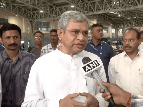
The foundation-laying project is being implemented by US-based 3D Glass Solutions (3DGS) through its wholly-owned Indian subsidiary, Heterogeneous Integration Packaging Solutions Private Limited. According to The Indian Express, global tech giants like Intel and Lockheed Martin are investors in the project, with Intel CEO Dr. Lip-Bu Tan attending the groundbreaking ceremony virtually. The total project investment is approximately INR 19.34 billion, approved under India's semiconductor initiative and receiving central government financial support. The project is expected to have an annual production capacity of 70,000 glass panels, 50 million assembly units, and around 13,000 advanced 3D heterogeneous integration modules, creating about 2,500 direct and indirect jobs.
3DGS will establish a vertically integrated advanced packaging and embedded glass substrate unit here, introducing next-generation packaging technologies such as glass interposers and 3D heterogeneous integration modules. Compared to traditional silicon-based packaging, glass substrates offer a lower dielectric constant, superior high-frequency signal integrity, and stronger thermal stability. The facility is designed to integrate three manufacturing stages—substrate fabrication, assembly, and advanced packaging—at a single site, differing from the traditional outsourced assembly and test model. Products will target high-growth application areas such as data centers, high-performance computing, Artificial Intelligence, machine learning, 5G/6G communication systems, photonics, automotive radar, and defense electronics.
Vishal Dev, Additional Chief Secretary of the Odisha Energy Department, stated at the ceremony that 3DGS's investors include Intel and Lockheed Martin. This is a significant development for Odisha's electronics and semiconductor ecosystem and will pave the way for further investment in the sector. Odisha is the only state in India to have both the first commercial compound semiconductor manufacturing unit and the first 3D glass substrate packaging facility. The state is accelerating its transformation from a traditional base for metals and minerals to a hub for high-end electronics manufacturing.
In addition to the 3DGS project, SiCSem, in collaboration with UK-based Clas-SiC Wafer Fab Ltd., will establish India's first commercial compound semiconductor manufacturing unit at Info Valley in Bhubaneswar. It will focus on silicon carbide device production, with an annual capacity of 60,000 wafers and a packaging capacity of 96 million units, serving the defense, electric vehicles, railways, and renewable energy sectors. The Indian central government has approved ten semiconductor projects nationwide, with cumulative investments exceeding INR 1.6 trillion, and Odisha hosts two of them. Vaishnaw stated that efforts will be made to double the capacity after the completion of the first phase, continuously advancing Odisha's industrialization process.
This article is compiled by Wedoany. All AI citations must indicate the source as "Wedoany". If there is any infringement or other issues, please notify us promptly, and we will modify or delete it accordingly. Email: news@wedoany.com