en.Wedoany.com Reported - Samsung Electronics' foundry division will expand its multi-project wafer (MPW) service to the 2-nanometer process starting next year. The 2-nanometer node is currently the most advanced commercially available process, and this move is expected to accelerate the development of ultra-high-performance artificial intelligence (AI) semiconductors by South Korean fabless companies.
Samsung Electronics Foundry Division Executive Director Song Tae-jung (송태중) announced this plan on the afternoon of the 15th at the "M.AX Alliance First Half General Meeting" held at EL Tower in Yangjae, Seoul.
MPW is a service where a foundry company places chips developed by multiple fabless firms on the same wafer for trial production. This model shares wafer costs, thereby reducing the development cost burden for fabless companies.
Samsung Electronics strengthens its foundry ecosystem annually through MPW services across various processes. Last year and this year, the most advanced process node offered by this service was 4 nanometers.
Starting next year, the MPW process will be expanded to 2 nanometers. The 2-nanometer node is the latest commercialized process in the foundry industry. Due to its high manufacturing difficulty, it is primarily used for ultra-high-performance semiconductors in areas such as AI and high-performance computing (HPC).
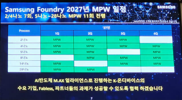
In terms of specific scheduling, the 2-nanometer and 4-nanometer processes will each undergo 7 MPW runs next year, while processes from 5 to 28 nanometers will undergo 11 MPW runs. If including the 8-inch process, which belongs to older nodes, the total frequency of MPW runs is expected to increase further.
Song Tae-jung stated that Samsung Foundry, under the name "SAFE," is working with the surrounding ecosystem to develop the most advanced processes. At the same time, through the AI semiconductor M.AX Alliance platform, it will fully support K-On-device demand companies, fabless firms, and partners in achieving their goals.
The M.AX Alliance First Half General Meeting was attended by over 150 people from demand companies, fabless firms, foundries, semiconductor IP companies, semiconductor industry associations, and the Korea Evaluation Institute of Industrial Technology (KEIT), representing both industry and government. The event focused on strategies to secure domestic AI chips, with an agenda that included a business agreement signing ceremony for the "Semiconductor Manufacturing Support TF" and a briefing session on the "K-On-device AI Semiconductor Technology Development Project."
This article is compiled by Wedoany. All AI citations must indicate the source as "Wedoany". If there is any infringement or other issues, please notify us promptly, and we will modify or delete it accordingly. Email: news@wedoany.com