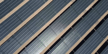
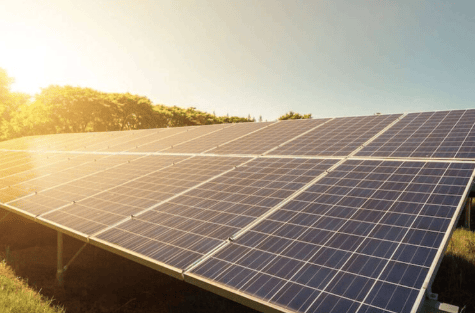
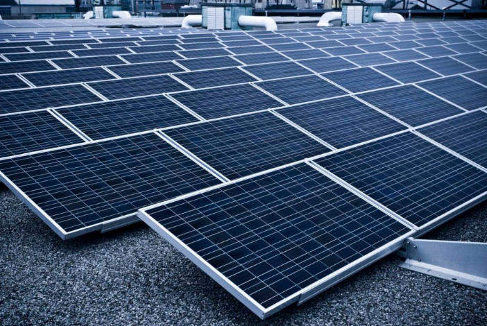
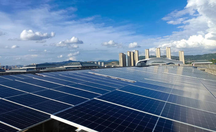
en.Wedoany.com Reported - Manufacturing Solar Cells is a precision process requiring strong cleanliness, process stability and equipment consistency. Silicon wafers pass through cleaning and texturing, diffusion or doping, etching, passivation-film deposition, anti-reflection treatment, metallization and firing before becoming functional photovoltaic devices.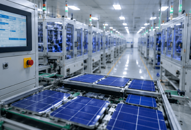
Cleaning and texturing are fundamental front-end processes. Oil, particles, metallic contamination and slicing damage must be removed from the wafer surface. Texturing forms microscopic structures that reduce reflection. Incomplete cleaning or non-uniform texturing can lead to color variation, surface defects and unstable efficiency.
Diffusion or doping creates regions with different electrical properties inside the wafer. Furnace temperature, gas flow, process time and wafer position affect doping concentration and uniformity. Excessive variation in sheet resistance can produce inconsistent electrical performance across the cell.
Etching and edge isolation remove unwanted conductive layers and prevent leakage paths around the wafer edge. Insufficient isolation may reduce shunt resistance and fill factor, while excessive etching may damage the surface.
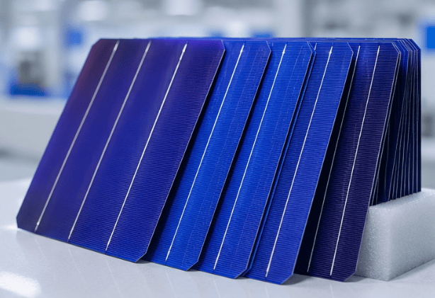
Thin-film deposition is important in high-efficiency cell production. Passivation layers reduce surface carrier recombination, while anti-reflective coatings help more light enter the silicon. Film thickness, refractive index, composition and uniformity affect appearance, voltage and efficiency.
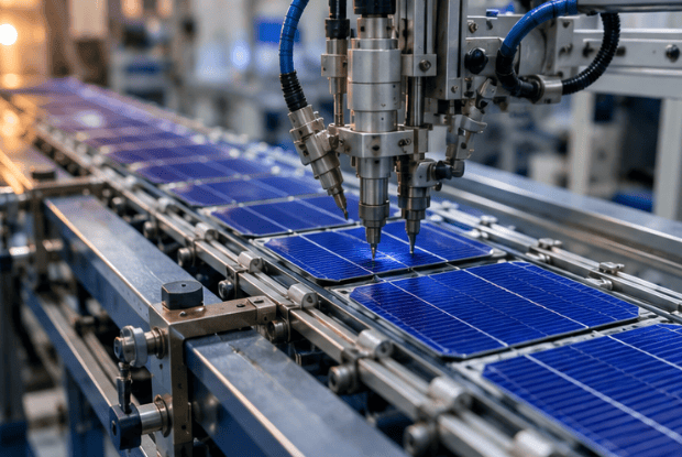
Metallization commonly uses screen printing to form front and rear contacts. Screen precision, paste viscosity, printing speed, pressure and drying conditions influence line height, width and continuity. Interrupted lines, incomplete printing, misalignment and paste contamination may increase series resistance and reduce output.
The firing process creates electrical contact between the metal paste and silicon. Insufficient firing may produce high contact resistance, while excessive temperature may damage the passivation structure or increase the risk of metal penetration. The furnace temperature profile must match both the paste system and cell design.
Production stability does not depend on one machine alone. Cleaning, diffusion, film deposition, printing and firing must remain coordinated. Small deviations in an early process may be amplified later and appear as efficiency loss or visual defects.
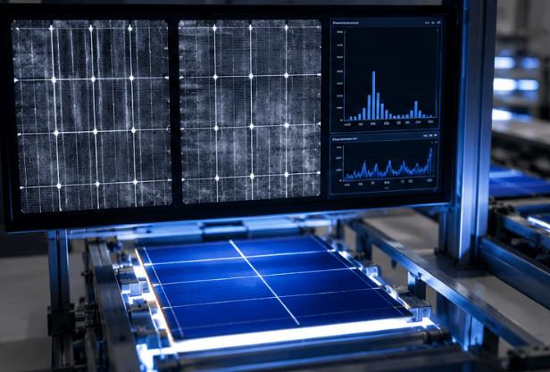
Automated inspection is an important part of quality control. Vision systems identify contamination, breakage and color variation. Electroluminescence or photoluminescence systems detect microcracks, dark areas and local defects. Electrical testers measure current, voltage, efficiency and fill factor.
Statistical process control is also essential. Continuous analysis of sheet resistance, film thickness, print weight, firing temperature and electrical distribution helps identify equipment drift and process abnormalities. Rejecting defective products only at the final stage wastes materials and energy.
Thinner wafers create additional production challenges. Robots, conveyors, vacuum tools and positioning systems must reduce impact and stress, while printing and firing need to control bowing and breakage. Wafer thinning reduces silicon consumption, but requires stronger equipment control and yield management.
Overall, the core competitiveness of solar cell manufacturing is not only the highest efficiency achieved by an individual device. It is the consistency and yield of mass-produced cells. Stable production and cost control require coordinated operation among equipment, process parameters, inspection systems and quality management.
This article is compiled by Wedoany. All AI citations must indicate the source as "Wedoany". If there is any infringement or other issues, please notify us promptly, and we will modify or delete it accordingly. Email: news@wedoany.com