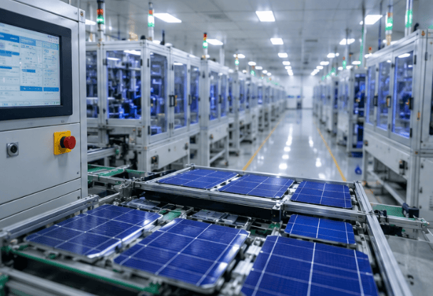
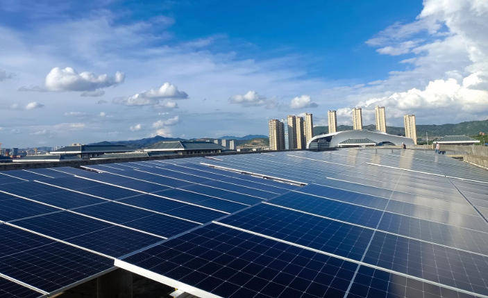
en.Wedoany.com Reported - As the photovoltaic industry continues to improve conversion efficiency and power output, Solar Cells are evolving toward high-efficiency structures such as TOPCon, heterojunction and back-contact designs. These technologies differ in wafer type, passivation structure, metallization, processing temperature, production equipment and module integration.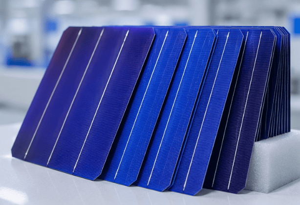
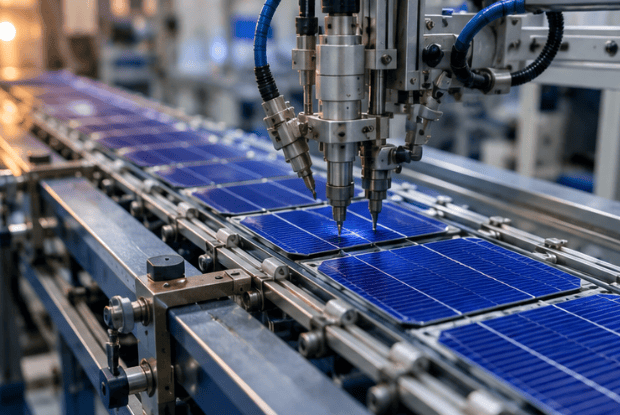
TOPCon cells normally use an ultra-thin tunneling oxide layer and a doped polysilicon layer to reduce carrier recombination and improve voltage performance. The technology can be developed from parts of the conventional crystalline silicon manufacturing base, but it places higher requirements on thin-film deposition, diffusion, cleaning and metallization.
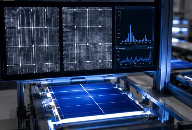
The tunneling oxide is extremely thin, making thickness uniformity and interface quality important. Non-uniform oxide, surface contamination or weak passivation may reduce selective carrier transport and cell efficiency. Uniform deposition and doping of the polysilicon layer also affect performance across the wafer.
Heterojunction cells combine a crystalline silicon wafer with amorphous silicon thin films to form passivated contacts. This structure provides strong surface passivation, high voltage potential and favorable temperature performance. The manufacturing process uses relatively low temperatures, but requires very clean wafer surfaces, uniform thin-film deposition and high-quality transparent conductive layers.
Heterojunction metallization must be compatible with low-temperature processing. Conductive paste resistance, adhesion, curing behavior and material consumption affect both cost and electrical performance. The transparent conductive layer must also balance conductivity with optical transmission.
Back-contact cells place most positive and negative contacts on the rear side of the device, reducing front-side shading from metal grid lines. This provides a clean front appearance and a larger light-receiving surface, making the structure suitable for applications that value high efficiency and visual uniformity.
However, back-contact designs normally require more complex patterning, doping and electrical isolation. Positive and negative contact regions must be arranged precisely to prevent short circuits and current losses. Module interconnection also needs to match the rear-contact layout.
All of these technologies require high-quality silicon wafers. Resistivity, minority-carrier lifetime, oxygen and carbon content, thickness uniformity and surface defects influence final performance. As wafers become thinner, mechanical strength and breakage control become increasingly important.
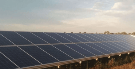
Bifacial power generation is another characteristic of some advanced cell designs. The rear side can receive reflected light and generate additional power, but actual gain depends on ground reflectance, module height, tilt angle, support structure and row spacing.
Technology selection should not be based only on laboratory efficiency. Equipment investment, production yield, material consumption, silver usage, thin-wafer capability, module compatibility and long-term reliability must also be considered. Higher efficiency may not create sufficient commercial value if manufacturing cost rises sharply or yield declines.
Overall, TOPCon, heterojunction and back-contact cells represent competition among complete material systems, manufacturing processes and module designs rather than efficiency alone. The technologies with the strongest long-term value will be those that combine high efficiency, strong yield, low material consumption and stable mass production.
This article is compiled by Wedoany. All AI citations must indicate the source as "Wedoany". If there is any infringement or other issues, please notify us promptly, and we will modify or delete it accordingly. Email: news@wedoany.com