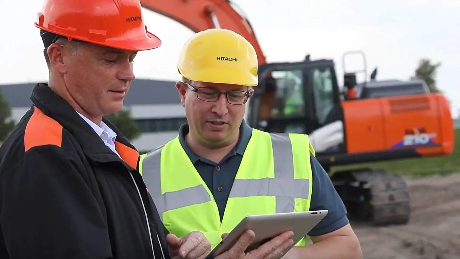
en.Wedoany.com Reported - TLB, a Korean PCB specialized company, announced on the 24th that it has signed a Memorandum of Understanding (MOU) with Company A, which possesses equipment and process technologies related to glass substrates, to enter the next-generation semiconductor packaging market based on glass substrates. The two parties will engage in joint development and technical cooperation in the fields of glass substrates and semiconductor packaging technology.
This MOU designates Through Glass Via (TGV) technology, metallization technology, and glass substrate manufacturing technology for semiconductor packaging as core cooperation topics. The two parties have decided to establish a full-cycle technical cooperation system, ranging from related materials, chemicals, and equipment review to trial production, performance and reliability evaluation. They also plan to jointly address domestic and international patents, certifications, and standardization efforts.
Based on their respective strengths, TLB, leveraging its business experience accumulated in semiconductor PCBs and next-generation packaging, will be responsible for market requirement review, technical evaluation, and commercialization feasibility analysis. Company A, based on its glass substrate-related equipment and process technologies, will be responsible for providing and reviewing technical information. The cooperation structure remains open, allowing for the subsequent inclusion of third-party research institutions or semiconductor material, component, and equipment companies in joint development projects.
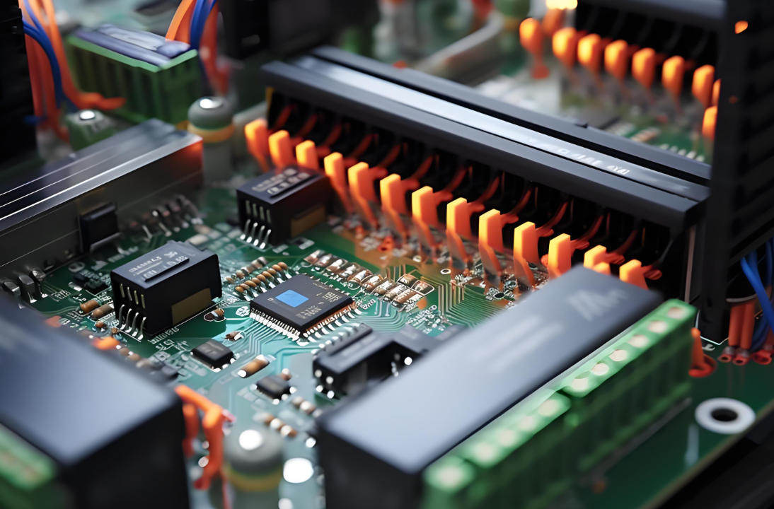
Glass substrates offer advantages over traditional organic substrates, such as lower signal loss and a lower coefficient of thermal expansion (CTE), and are considered a next-generation material for high-performance AI semiconductors and High Bandwidth Memory (HBM) packaging. As global companies accelerate commercialization, Korean PCB companies are also actively positioning themselves in the glass substrate market.
TLB is a specialized memory semiconductor substrate company whose main clients include SK Hynix, Samsung Electronics, and Micron. This cooperation aims to extend its PCB technical capabilities into the field of glass substrate packaging.
A TLB official stated that this MOU is a preemptive response to next-generation semiconductor packaging trends, with the goal of translating joint R&D results into actual business.
This article is compiled by Wedoany. All AI citations must indicate the source as "Wedoany". If there is any infringement or other issues, please notify us promptly, and we will modify or delete it accordingly. Email: news@wedoany.com