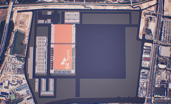
en.Wedoany.com Reported - GigaLane (기가레인) has successfully leveraged AI technology to automatically derive optimal conditions for the plasma etching process, transforming the process development method, which previously relied on engineer experience and repeated experiments, into a data-driven model. The company is led by CEO Kim Hyun-je (김현제) and specializes in the field of semiconductor etching equipment.
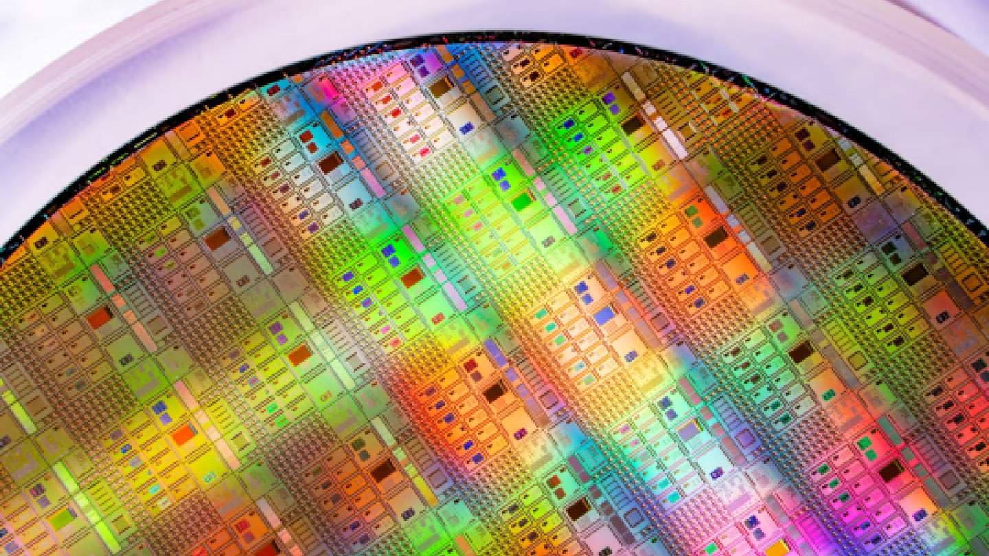
The etching process is a core step in semiconductor manufacturing, where plasma is used to precisely remove unnecessary parts from the wafer to form circuit patterns. As semiconductors become more miniaturized and highly integrated, the number of variables engineers need to control has increased exponentially. These include multiple input parameters such as pressure, source power, bias power, gas type and the injection amount of each gas, chuck temperature, backside helium, and process time. At the same time, the process results must meet six target indicators: etch amount, etch rate, etch angle, top and bottom critical dimensions, and mask selectivity. Due to the large number of variables and stringent requirements, engineers typically need to repeatedly conduct numerous tests to find the optimal conditions, which is time-consuming and consumes a large number of wafers.
To address this inefficiency, GigaLane, with support from the National Research Council of Science and Technology's Convergence Research Group project, adopted an AI process optimization tool independently developed by the Plasma Equipment Intelligence Research Group of the Korea Institute of Fusion Energy. The research team input 34 refined data points, obtained after removing outliers from 51 experimental data points executed by engineers, into the AI model for learning. After just one learning session, the AI successfully derived optimal conditions that simultaneously satisfied all six process targets. If the optimal conditions were not achieved in a single learning session, the system also built a repetitive algorithm that inputs new process results for further learning and proposes new optimal conditions, thereby further increasing the success rate of process development. This approach significantly reduces the wafers and engineering resources required for process optimization while accelerating the response time to diverse customer needs.
Based on this achievement, GigaLane plans to expand the application of AI to other processes, creating a virtuous cycle where greater data accumulation leads to higher development efficiency. The company will also advance from the current stage of "matching input variables with result values" to a higher level, linking real-time sensor data generated by equipment during the process with AI to build a "self-operating equipment" system where semiconductor equipment can diagnose and correct process conditions on its own. A GigaLane representative stated that, based on this data-driven process optimization workflow, the company will efficiently respond to the needs of global semiconductor device companies and enhance its market competitiveness.