Micron Begins Expansion of Hiroshima Wafer Fab in Japan, Investing $9.3 Billion in HBM
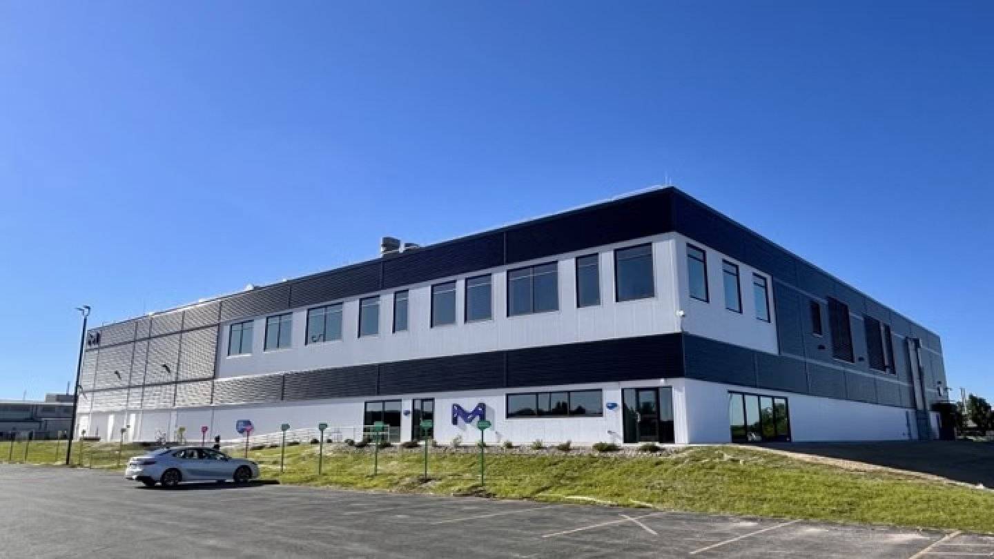
en.Wedoany.com Reported - On July 4, local time, Micron Technology of the United States commenced the expansion of its wafer fab in Hiroshima, Japan, with a total project investment of approximately 1.5 trillion yen, equivalent to about $9.3 billion. The project will be used to produce advanced memory chips such as high-bandwidth memory, primarily targeting AI processor demand, with related products expected to begin shipping around the summer of 2028.
High-bandwidth memory is a key storage component in AI servers and AI accelerators, often co-packaged or working in tandem with processors such as GPUs and AI ASICs to enhance data transfer bandwidth and model computing efficiency. As the scale of large model training, inference, and data center clusters expands, HBM supply capacity has become a critical constraint in the AI chip industry chain. Micron's expansion of advanced storage capacity in Hiroshima is not aimed at ordinary consumer-grade storage expansion, but at building storage capabilities for AI processors, data center servers, and next-generation high-performance computing platforms.
Japan's Ministry of Economy, Trade and Industry will provide up to approximately 500 billion yen in subsidies to support the project. For Japan, introducing Micron to expand HBM and advanced DRAM production helps strengthen the domestic semiconductor manufacturing base and enhance Japan's participation in the global AI hardware supply chain.
Micron's Hiroshima plant has long been responsible for the company's advanced DRAM manufacturing. After this expansion, it will further take on the production of AI storage products. HBM manufacturing imposes high requirements on wafer processes, stacking packaging, yield control, testing capabilities, and customer certification, and simply increasing factory floor space does not immediately translate into effective production capacity. The timeline from groundbreaking to shipping around the summer of 2028 indicates that the construction cycle will cover multiple stages, including factory expansion, equipment installation, process validation, customer certification, and production ramp-up. For AI chip customers, the release of new HBM capacity is expected to alleviate some of the supply tightness for high-end storage, but the actual impact on market supply will also depend on yield rates, product generations, packaging support, and customer order pacing.
This project is also part of Micron's global AI storage capacity expansion plan. In addition to Hiroshima, Japan, Micron is advancing large-scale advanced process investments in Idaho and New York in the United States to boost DRAM and HBM supply capabilities. As Nvidia, AMD, cloud service providers, and AI chip companies continue to increase demand for high-performance storage, global memory manufacturers are competing in capacity and technology around HBM3E, HBM4, and subsequent products. With the Hiroshima project underway, Micron will simultaneously advance its AI storage capacity layout in Asia and the United States, forming a more distributed manufacturing network.
Currently, the project has officially broken ground, with the investment scale, subsidy arrangements, and initial shipping timeline already confirmed. The next focus will shift to equipment arrival, process introduction, HBM product validation, customer certification, and production ramp-up progress after 2028.
Keywords: Micron Technology, Hiroshima Wafer Fab, HBM, AI Memory Chips, 1.5 Trillion Yen
Related Products

20 Inch 1600*900 Full HD 60Hz TFT LED Monitor with VGA and DP Interfaces for Desktop Computers-Business Use
Guangzhou Zanying Optoelectronics Technology Co., Ltd.
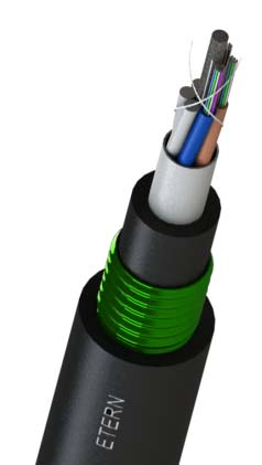
GYTA Type Non-Self-Supporting Aerial/Duct Optical Cable
TONGDING INTERCONNECTION INFORMATION CO., LTD.
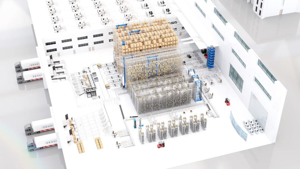
One-Stop Steward Service for the Entire Logistics System Integration Chain
Zhongding Intelligent (Wuxi) Technology Co., Ltd.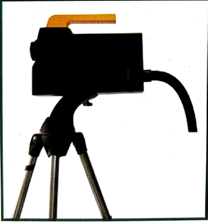
Automatic Aiming Laser Remote Obstacle Removal Robot
Pinggao Group Weihai High-Voltage Apparatus Co., Ltd.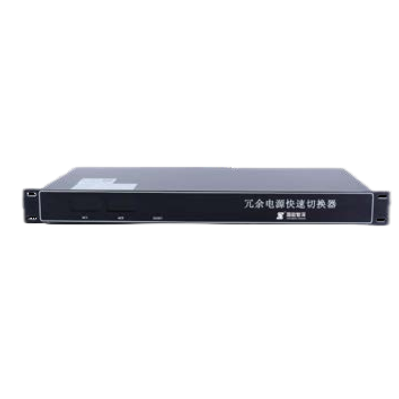
TWP16 P-Band Tropospheric Wind Profile Radar
China Huayun Meteorological Technology Group Co., Ltd.

Multi-function Marine Monitoring Low-altitude Detection Radar Sea-air Boundary Ocean Dynamic Environment Measurement
Chengdu Dixin Technology Co., Ltd.