Intel Files Cross-Batch Memory Patent Using Back-End Transistors and UCIe Interface
en.Wedoany.com Reported - Intel has proposed a new high-bandwidth memory architecture called Cross-Batch Memory (XBM) in a patent application. The technology uses back-end transistors and a UCIe serial interface to achieve chip-native integration at lower cost, with module package dimensions targeting alignment with the HBM4 standard. The patent was filed on December 26, 2024, and published on July 2, 2026, solely by Intel, representing a different technical path from the ZAM project developed in collaboration with SoftBank.
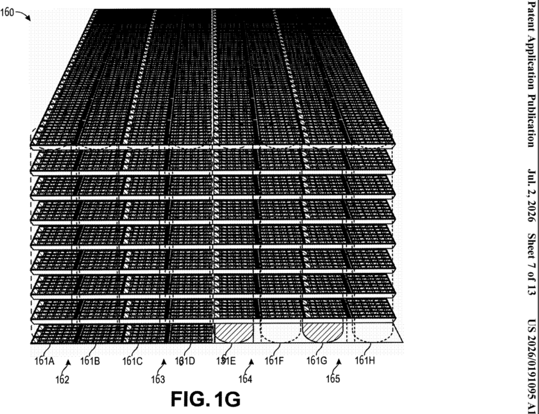
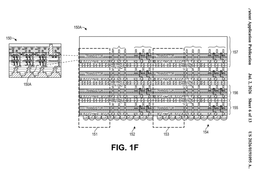
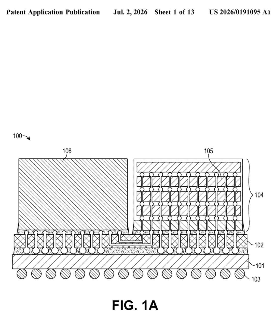
The basic design of XBM replaces the traditional 1024-bit ultra-wide parallel interface used in HBM with a 32 GT/s UCIe link, eliminating the need for expensive silicon interposers, reducing package size, and lowering packaging complexity. The design uses a base die at the bottom of the stack for serialization and signal transmission, referred to as a "chip-native" approach. The core change in the XBM memory stack lies in the memory cell structure: traditional DRAM transistors are etched into the front-end silicon layer at the bottom of the chip, while XBM moves the 1T1C (one transistor, one capacitor) cell to the back-end metal stack layer, manufactured using thin-film transistor technology. Each chip has a capacity of approximately 1.5 GB, containing 768 data blocks arranged in a 32×24 grid, divided into 8 channels, each further divided into 8 sub-channels, with a stack height of 8 layers expandable to 16 layers. All memory chips are bonded together through through-silicon via "trenches" and double-sided high-bandwidth interconnects.
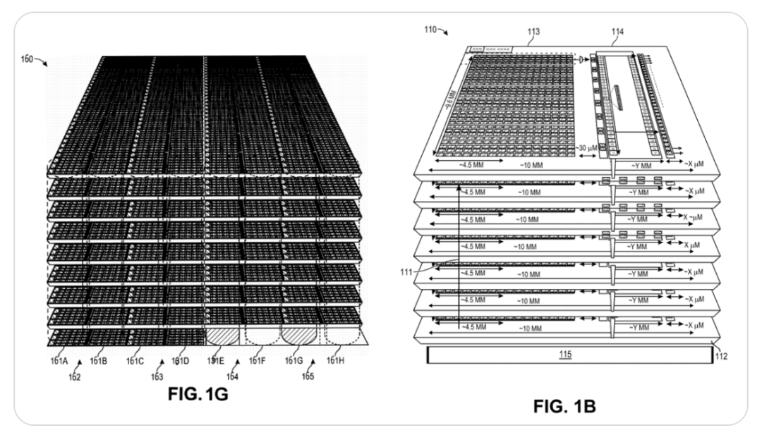
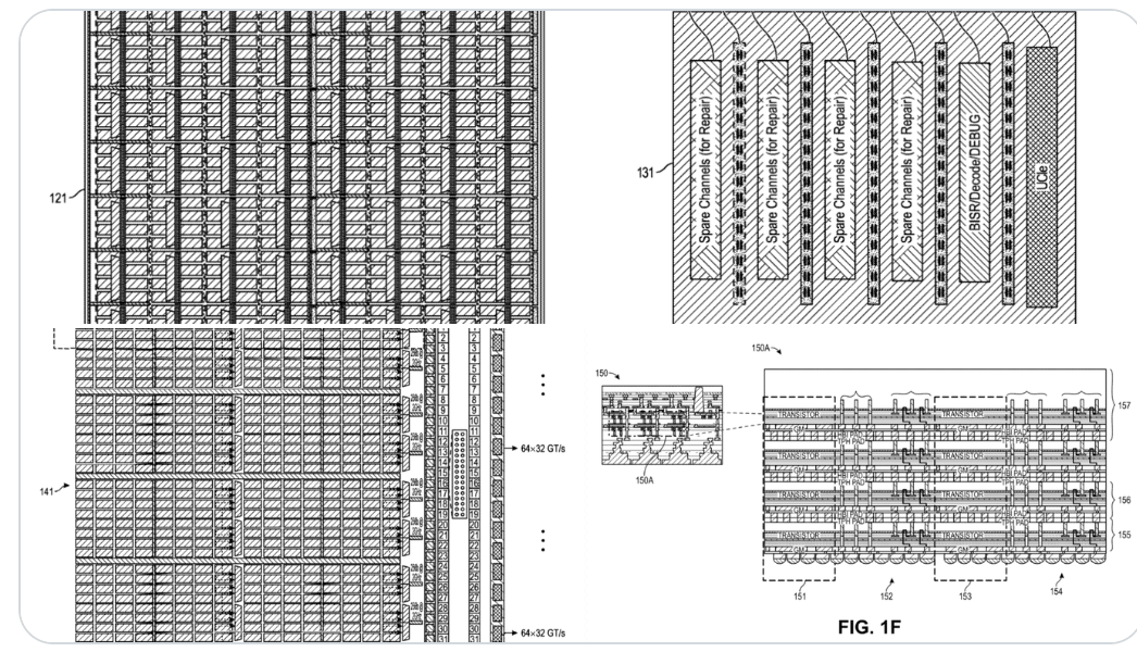
Intel emphasized repairability design in the patent. The base die is equipped with dedicated spare channels, built-in self-repair logic, and four redundant memory array sub-channels, which can be used to replace defective cells in upper chips after stack assembly. This "post-assembly repair" mechanism aims to improve the overall yield of ultra-high stack chips.
Further content of the patent application focuses on packaging methods. Intel describes a packaged memory and "reverse overhang" structure designed to reduce the Z-axis height of the stack—traditional packaged memory adds 300 to 350 micrometers—while eliminating stiffeners used for warpage control and directly powering the DRAM from the voltage regulator.
The strategic significance of moving DRAM cells to the back-end is that back-end transistors deposited in low-temperature metal lines do not require the front-end silicon processes of dedicated DRAM fabs. Foundries with logic and advanced packaging capabilities could, in principle, manufacture HBM-grade memory through their own production lines. Currently, global DRAM is produced by three companies: SK Hynix, Samsung, and Micron, with SK Hynix holding approximately 60% of the HBM market share. If back-end transistor technology achieves viable yield and density, it could theoretically open a fourth HBM manufacturing path.
However, the patent is currently only a published patent application, not a granted patent or actual product, and the document does not mention specific bandwidth or yield data. XBM should not be confused with the ZAM architecture jointly developed by Intel and SoftBank subsidiary SAIMEMORY. ZAM uses fusion bonding technology to stack nine layers of DRAM, with inter-layer silicon thickness of approximately 3 micrometers, reportedly offering about twice the bandwidth density of HBM4, with plans to be showcased at the 2026 VLSI Symposium and a commercialization target of 2029. XBM is a separate application filed by Intel, altering both the DRAM transistors themselves and their interface.
In terms of limitations, the UCIe interface used by XBM currently reaches the specification ceiling of 32 GT/s data rate, with no significant room for performance improvement. The mass production capability of back-end transistor DRAM has not been publicly verified, and the capacitor in the 1T1C cell is the most difficult component to scale down in DRAM. The project moves it to the back-end rather than removing it, and back-end capacitors under HBM density and yield conditions remain an unachieved step. Meanwhile, SK Hynix, Samsung, and Micron are each advancing their own 3D-DRAM projects, with SK Hynix targeting product launch around 2030.
Intel sold its NAND flash memory business to SK Hynix in 2021 and ceased production of the Optane memory product line in 2022. Although the company does not sell HBM products, this patent application indicates it is still exploring new memory architectures. In the ZAM project co-developed by Intel and SoftBank, the actual DRAM manufacturing is handled by Powerchip, not Intel itself.
Related Products


GYTA Type Non-Self-Supporting Aerial/Duct Optical Cable
TONGDING INTERCONNECTION INFORMATION CO., LTD.
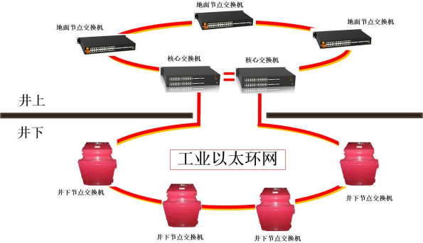
Mine Explosion-proof and Intrinsically Safe Industrial Ethernet Ring Network (10 Gigabit/Gigabit)
Chongqing Mas Sci&Tech Co., Ltd.

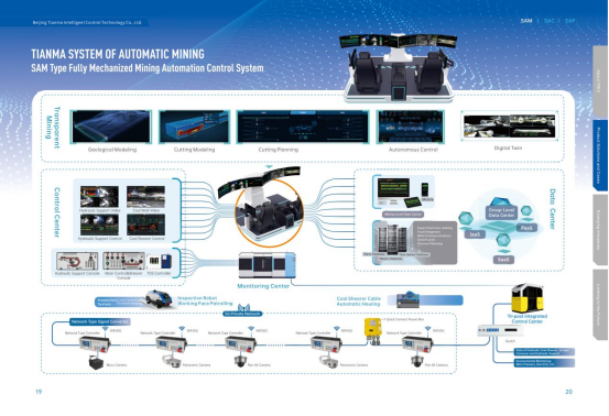
Comprehensive Mining Automation Control System
Beijing Tianma Intelligent Control Technology Co., Ltd.

Multi-function Marine Monitoring Low-altitude Detection Radar Sea-air Boundary Ocean Dynamic Environment Measurement
Chengdu Dixin Technology Co., Ltd.
MUX Series Communication Interface Device for Security and Stability Control System
Nanjing NR Electric Co., Ltd.
Automatic Aiming Laser Remote Obstacle Removal Robot
Pinggao Group Weihai High-Voltage Apparatus Co., Ltd.