TSMC's PIC Monthly Capacity in Taiwan, China to Expand to 10,000 Wafers
en.Wedoany.com Reported - TSMC's silicon photonics PIC capacity is set to expand rapidly, with analysts estimating that its monthly capacity will increase from the current approximately 500 wafers to 10,000 wafers per month by the second quarter of 2026, further rising to 15,000 wafers in the fourth quarter, and reaching at least 25,000 wafers per month by 2028. PIC is the core component of CPO optical engines, responsible for the conversion, guidance, and coupling of electrical and optical signals. As AI server clusters expand, switch bandwidth advances from 25T and 50T to 100T and 200T, driving corresponding growth in demand for optical engines, making the progress of TSMC's COUPE platform a focal point of market attention.
According to analyst estimates, based on 648 dies per wafer, after TSMC's PIC monthly capacity increases from 500 wafers to 10,000 wafers, the annualized PIC output could rise from approximately 4 million units to 78 million units; if capacity further reaches 25,000 wafers per month, the annualized PIC output could reach 194 million units. Assuming a SoIC yield of 50%, the optical engine output would be approximately 2 million, 39 million, and 97 million units, respectively; further incorporating downstream assembly yields, the actual optical engine shipments are estimated at approximately 390,000, 7.78 million, and 48.6 million units, respectively. Due to limited PIC resources in the early stages, the main volume production customers for TSMC's COUPE platform from 2026 to 2027 are likely to be NVIDIA, Broadcom, and AMD; as capacity further expands by 2028, CPO projects from customers such as MediaTek, Marvell, and Ayar Labs may also enter TSMC's volume production platform. However, an increase in PIC capacity does not equate to an immediate full-scale ramp-up of CPO, as the backend still requires multiple stages including SoIC integration, optoelectronic testing, optical engine packaging, FAU coupling, and system-level verification. Analysts point out that TSMC's PIC capacity expansion carries three major implications. First, it signifies that CPO is transitioning from experimentation and small-scale validation to the production preparation phase; second, the combination of silicon photonics with advanced packaging will enable COUPE, SoIC, and CoWoS to form a more complete AI optoelectronic integration platform; third, the ramp-up of PIC will simultaneously drive demand for FAU, lasers, optical testing, probe cards, test sockets, and automation equipment.
As GPU designs evolve toward denser inter-chip connections and faster data transfer rates, global wafer foundry giants are increasingly entering the silicon photonics field. TSMC's COUPE silicon photonics platform is expected to achieve volume production by 2026, marking a critical step in the deployment of co-packaged optics (CPO). COUPE utilizes SoIC-X chip stacking technology, placing electronic chips directly atop photonic chips, achieving ultra-low impedance and higher energy efficiency at the inter-chip interface compared to traditional stacking methods. The technology roadmap aims to complete certification for small-form-factor pluggable devices in 2025, followed by CoWoS-based CPO integration in 2026. TSMC claims that COUPE achieves a 5 to 10 times improvement in power efficiency, a 10 to 20 times reduction in latency, and a more compact footprint through its interposer-based integration architecture. Shang Hou, Director of Advanced Packaging Integration at TSMC, stated that COUPE technology enables heterogeneous integration of electronic and photonic integrated circuits and plans to achieve volume production this year. He also highlighted three key challenges for the large-scale application of CPO: wafer-level testing, fiber array unit integration, and high-speed optical packaging assembly.
Advancing CPO development hinges on collaborative innovation across the entire supply chain. In addition to TSMC, global companies such as Coherent and Sumitomo Electric also provide key materials and laser technologies, while testing equipment leader Advantest is also developing silicon photonics solutions. Samsung's foundry business has officially entered the silicon photonics field, planning to launch an optical engine based on thermal compression bonding technology in 2027, followed by a turnkey co-packaged optics service in 2029. The plan was announced on March 17 at the 2026 Optical Fiber Communication Conference. Samsung's platform will utilize 300mm wafer processes for initial production. In the early stages, Samsung will focus on photonic integrated circuits, with potential customers including optical module manufacturers such as Coherent and Lumentum, as well as fabless companies developing their own PICs. Samsung Foundry also emphasized its vertically integrated memory capabilities. Unlike TSMC, which does not produce memory and relies on customers for external HBM procurement, Samsung highlighted its ability to offer HBM, foundry services, advanced packaging, and silicon photonics technology on a single vertically integrated platform.
Related Products

Automatic Aiming Laser Remote Obstacle Removal Robot
Pinggao Group Weihai High-Voltage Apparatus Co., Ltd.
Comprehensive Mining Automation Control System
Beijing Tianma Intelligent Control Technology Co., Ltd.
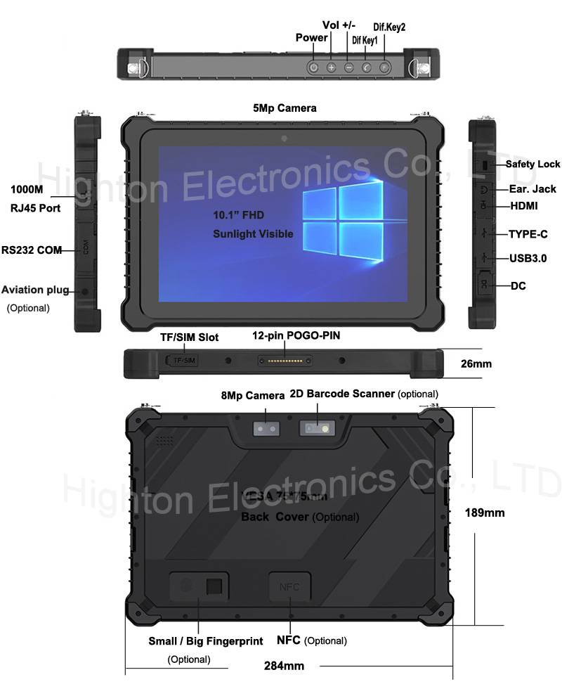
Hot Selling 10 Inch Intel N5100 I5 I7 FHD 8 +128GB 16+256GB Win10 Pro Win11 Pro 4G 5G Rugged Tablet PC Pad with NFC Barcode
Highton Electronics Co., Ltd.


TWP16 P-Band Tropospheric Wind Profile Radar
China Huayun Meteorological Technology Group Co., Ltd.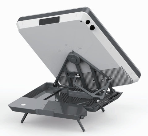
Flat Portable Satellite Terminal 0.35m Aperture Manual Portable Terminal
China Starwin Science & Technology Co., Ltd.